Solid state imaging device, method of driving solid state imaging device and image pickup apparatus

a solid-state imaging and pickup apparatus technology, applied in the direction of instruments, television systems, television system scanning details, etc., can solve problems such as difficulties in signal-to-noise ratio, and achieve excellent signal-to-noise ratio

Active Publication Date: 2006-11-02
SONY SEMICON SOLUTIONS CORP
View PDF2 Cites 29 Cited by
  • Summary
  • Abstract
  • Description
  • Claims
  • Application Information

AI Technical Summary

Benefits of technology

[0018] According to an embodiment of the invention, in the column signal processing circuit part having the analog amplifier, the feedback capacitance of the analog amplifier is used to do pixel addition, and thus the signals of the pixels can be amplified while the addition process can be done. Therefore, a pixel addition signal excellent in the signal-to-noise ratio can be obtained.

Problems solved by technology

However, in the related art above, the addition / averaging process for information about pixels having a filter in the same color in the unit pixel block is done in the stage in which pixel information is read out to a horizontal signal line, and thus noise components that can be added in a signal process system from pixels to the horizontal signal line also experience addition / averaging, which causes difficulties on the signal-to-noise ratio.

Method used


Image

  • Solid state imaging device, method of driving solid state imaging device and image pickup apparatus
  • Solid state imaging device, method of driving solid state imaging device and image pickup apparatus
  • Solid state imaging device, method of driving solid state imaging device and image pickup apparatus

Examples


Embodiment Construction

[0029] Hereinafter, an embodiment according to the invention will be described in detail with reference to the drawings.

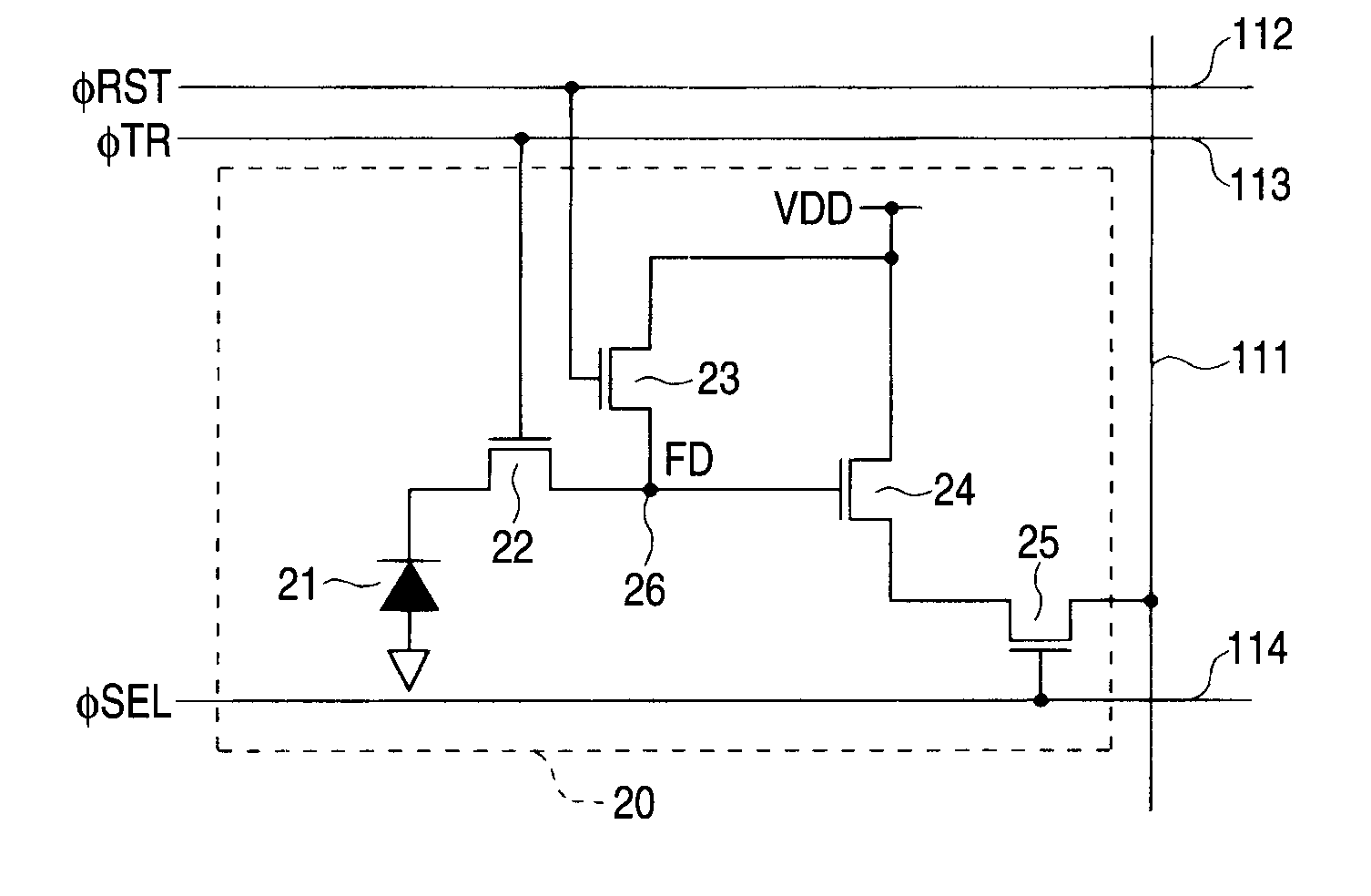
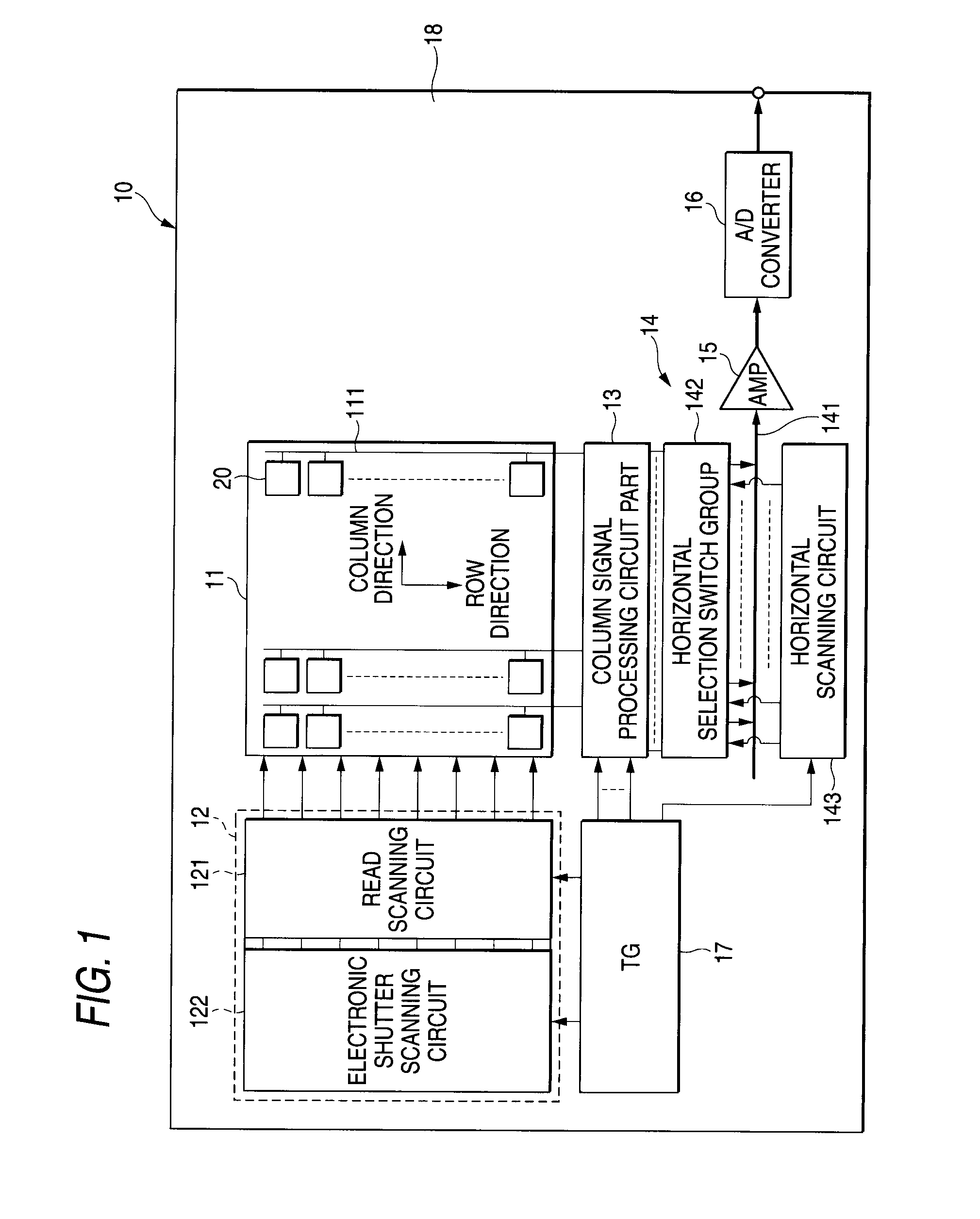
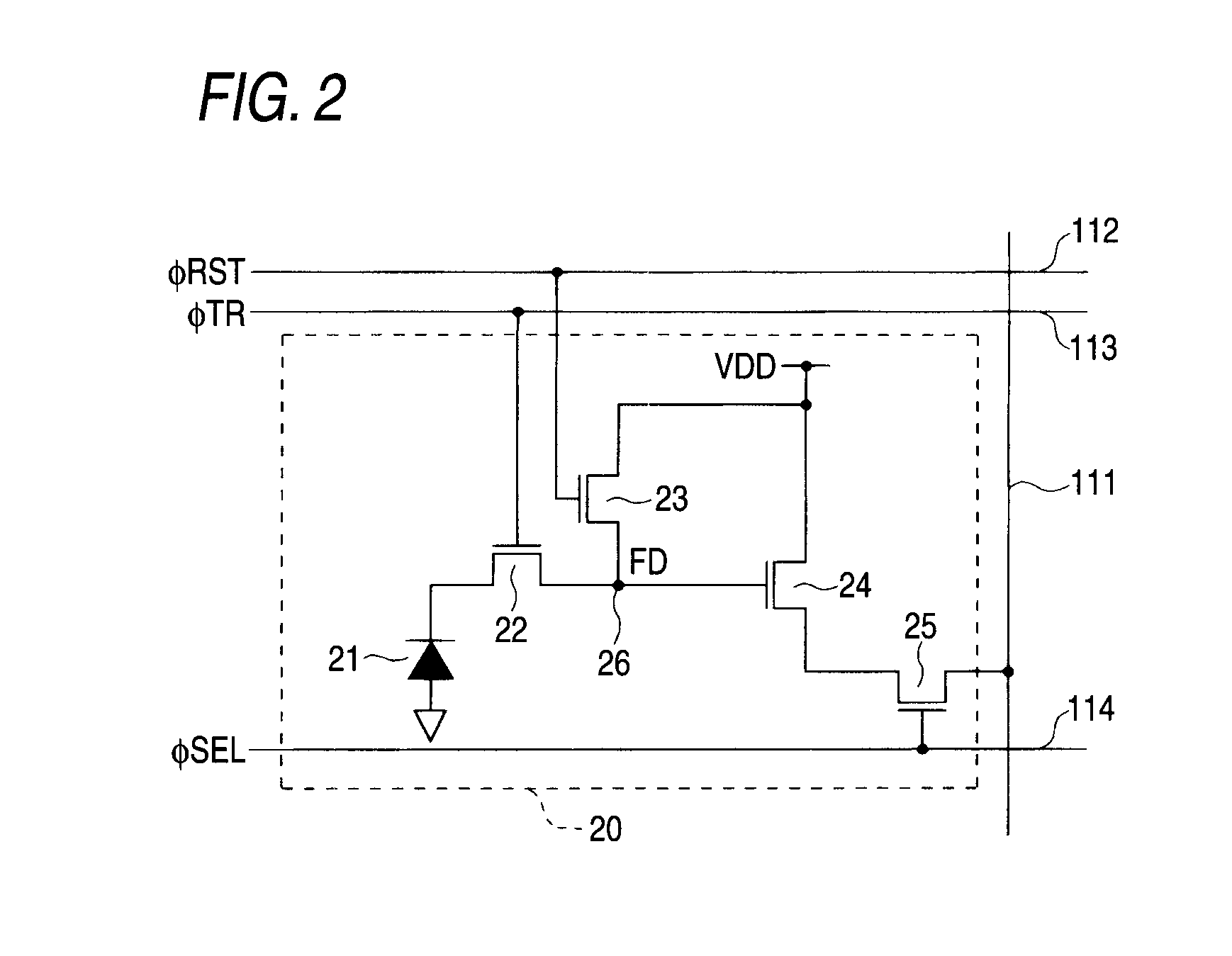
[0030]FIG. 1 is a block diagram illustrating the overall configuration of a solid state imaging device according to an embodiment of the invention, for example, an X-Y addressing solid state imaging device typified by a CMOS image sensor. As shown in FIG. 1, a solid state imaging device 10 of the embodiment has a pixel array part 11 as well as peripheral circuits including a vertical drive part 12, a column signal processing circuit part (column signal processing circuit part) 13, a horizontal drive part 14, an analog amplifier 15, an A / D converter 16, and a timing generator 17, and the device has the configuration in which these peripheral circuits are formed on a semiconductor substrate (chip) 18 as the pixel array part 11 is.

[0031] However, it is not limited to the configuration in which all the peripheral circuits are necessarily formed on the semiconductor s...


PUM


Abstract

When an addition/averaging process is done for pixels in the same color in a unit pixel block in a stage reading pixel information to a horizontal signal line, the addition/averaging process is also done for a noise component added in a signal process from the pixels to the horizontal signal line. Thus, a problem arises in the signal-to-noise ratio. Each of signal processing circuits of a column signal processing circuit part is provided with reverse amplifiers which output signals of pixels transmitted by a vertical signal line at a low impedance, and with feedback capacitances which are adjustably connected in parallel to these reverse amplifiers, the signal processing circuit being disposed at every column. These feedback capacitances are used to do row wise and column wise pixel addition for the pixels in the same color in the unit pixel block to take out pixel signals for a single pixel in simulation.

Description

CROSS REFERENCE TO RELATED APPLICATIONS [0001] The present invention contains the subject matter related to Japanese patent Application JP 2005-127631 filed in the Japanese Patent Office on Apr. 26, 2005, the entire contents of which being incorporated herein by reference. BACKGROUND OF THE INVENTION [0002] 1. Field of the Invention [0003] The present invention relates to a solid state imaging device, a method of driving a solid state imaging device and an image pickup apparatus. [0004] 2. Description of the Related Art [0005] A solid state imaging device is broadly divided into a charge transfer solid state imaging device typified by a CCD (Charge Coupled Device) image sensor, and an X-Y addressing solid state imaging device typified by a MOS (Metal Oxide Semiconductor) image sensor. In recent years, the latter solid state imaging device, for example the MOS image sensor is mounted particularly for use in a low power consumption camera module for mobile appliances such as a cellula...

Claims


Application Information

Patent Timeline
Patent Type & Authority Applications(United States)
IPC IPC(8): H01L27/00H04N5/335H04N5/341H04N5/347H04N5/357H04N5/369H04N5/372H04N5/374H04N9/07
CPCH04N5/347H04N9/045H04N5/378H04N5/3575H04N25/46H04N25/616H04N25/75H04N25/134
Inventor YAHAZU, KOJIYOKOTA, KAZUHIDEKOSEKI, KEN
Owner SONY SEMICON SOLUTIONS CORP
Why Eureka
Try Eureka