Inspection method and apparatus for partially drilled microvias

a micro-via and inspection method technology, applied in the direction of inspection/indentification of circuits, instruments, printed circuit manufacture, etc., can solve the problems of micro-via when plated or filled with a conductor shortening or electrical failure once the product is sold, and achieve the effect of improving the signal-to-noise ratio

Active Publication Date: 2008-06-19
HITACHI SEIKO LTD
View PDF15 Cites 11 Cited by
  • Summary
  • Abstract
  • Description
  • Claims
  • Application Information

AI Technical Summary

Benefits of technology

[0010]The present invention describes that the use of coaxial illumination in conjunction with off axis_provides a means to further differentiate the bulk surrounding material form the area being inspected.
[0011]The invention also emphasizes the tailoring of the coaxial illumination to illuminate the conductor pad or the selected area to be inspected. This type of selective illumination provides a better signal to noise ratio, since the surrounding bulk material is limited in illumination and will not add to the signal. The present invention also provides for the simultaneous use of multiple wavelength which can simultaneously enhance various features to further isolate the defects for proper inspection and analysis.

Problems solved by technology

When AOI is applied to the task of inspecting a laser microvia that is 50 microns in diameter and below, standard AOI systems fail to perform.
Standard AOI equipment lack the resolution and capability to differentiate the conductor pad which is supposed to be exposed and free from any contaminants, when the top dielectric is removed as the laser beam drills down to the conductor pad.
If the AOI system fails to find partially removed dielectric at the bottom of a microvia, even the slightest amount of dielectric film or resin, the microvia when plated or filled with a conductor will short or electrically fail once the product is delivered to clients.
Standard AOI systems are limited in the viewing of microvias, since microvias typically have diameters down to 10 microns.
This leaves few options for lighting and differentiating these thin films.
In many cases the AOI systems do not even detect the thin film that can be a thin as 1 micron.
In short the AOI systems have an unacceptable rate of false positives which leads to yield issues once more value is added to the multilayered printed circuit board or flex circuit.
In the case of high density chip packaging, one failure could cause serious failures in the field if the microvia is partially drilled.
In many cases next generation chip packaging will have nearly 40,000 microvias per chip package, only a few faulty microvias can ruin a product.

Method used


Image

  • Inspection method and apparatus for partially drilled microvias
  • Inspection method and apparatus for partially drilled microvias
  • Inspection method and apparatus for partially drilled microvias

Examples


Embodiment Construction

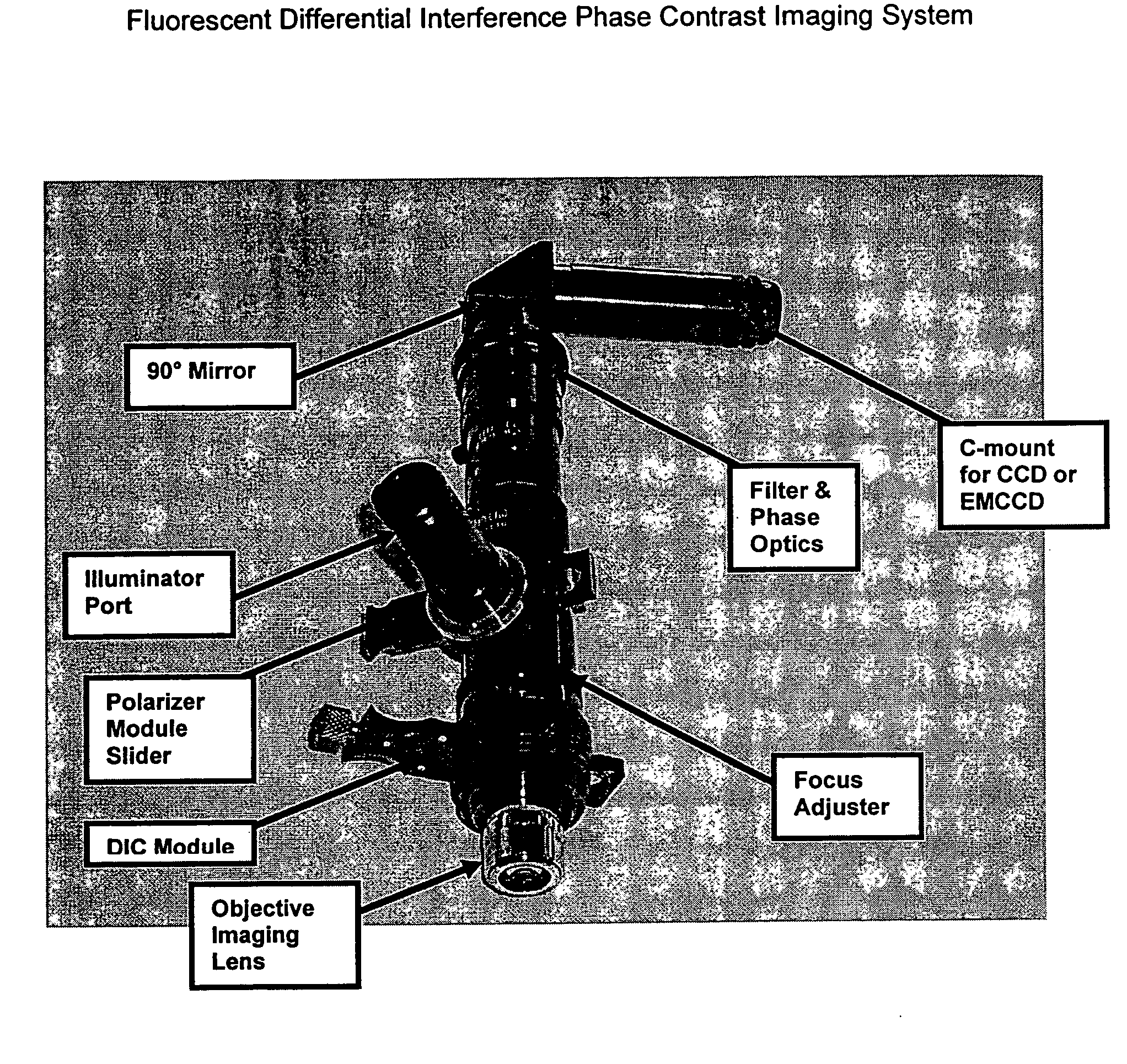
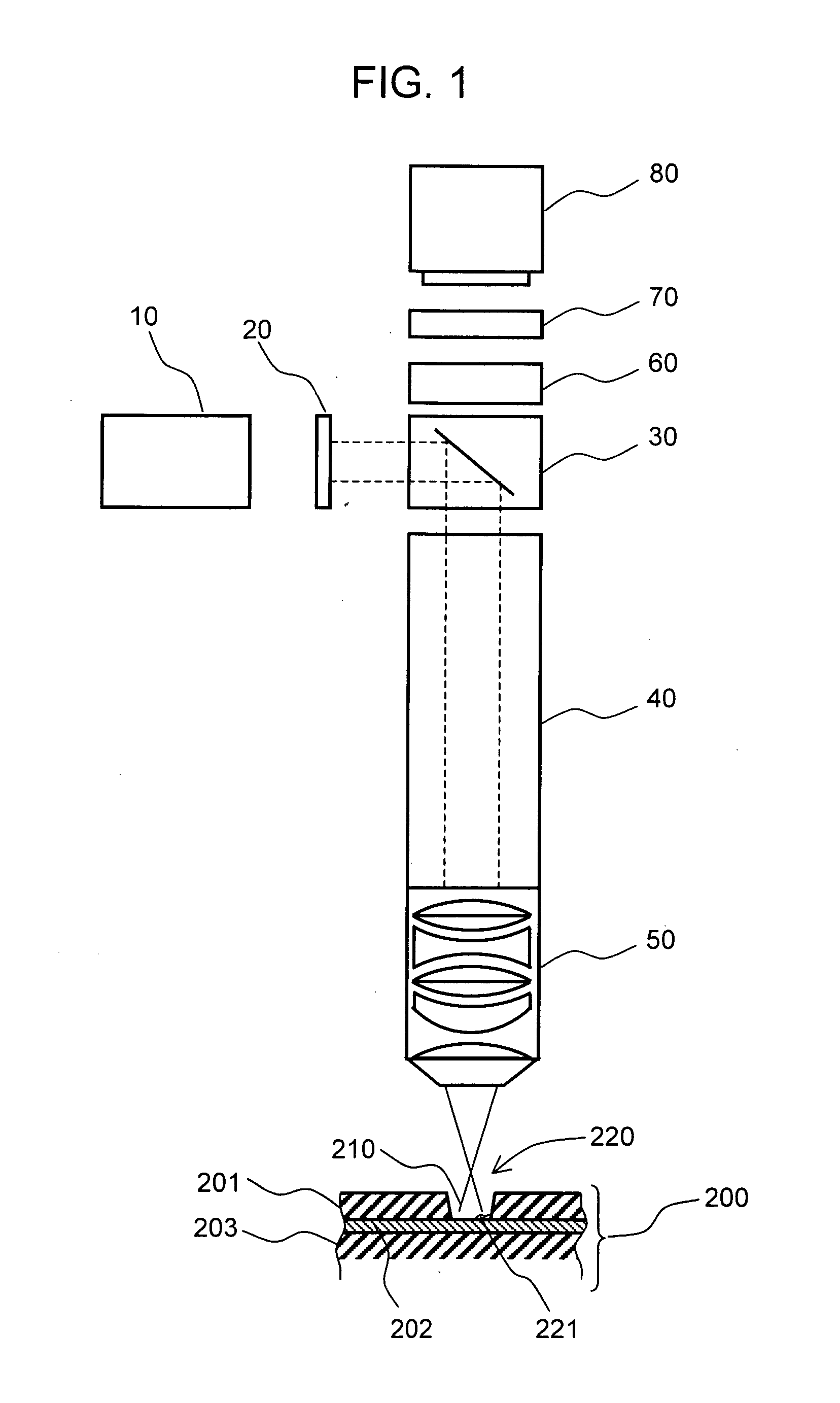
[0038]FIG. 1 shows a basic system that can image the defects by the use of the fluorescence emission.

[0039]The first approach uses a standard CCD and / or an EMCCD (hereinafter, simply referred to as “CCD”) 80. The use of a EMCCD or a L3CCD “Low Light Level CCD” provides a means to image very low fluorescent emissions from polymers being illuminated by an appropriate excitation wavelength. This system is optimized for higher sensitivity, faster speed, enabling lower concentrations of emitting molecules to be detected with shorter exposure times and lower excitation powers. The CCD 80 is coupled to a series of optical elements (filters) 70 including a UV filter or a specific filter for the illuminator wavelength or a stack of filters to isolate the wavelength of light being emitted by the polymer being illuminated.

[0040]The next stage is conditioning optics 60 to transfer the image to the CCD 80. This optic provides added capability to condition the image formed by the emission of fluo...


PUM


Abstract

Inspection of partially drilled microvias by fluorescence based optical imaging techniques, selective coaxial illumination and multivariable off-axis illumination and the use of comparative image analysis and the transformation of back reflected radiation by means of an integrated fluorescing plate mounted to the surface of a CCD or EMCCD array.

Description

CROSS REFERENCES TO RELATED APPLICATIONS[0001]The present Application is related to and claims benefit of Provisional Patent Application Ser. No. 60 / 674,752 filed Apr. 26, 2005 by Todd E. Lizotte and Orest P. Ohar.FIELD OF THE INVENTION[0002]The present invention relates to a method and an apparatus for inspection of partially drilled microvias by fluorescence based optical imaging techniques, selective coaxial illumination, multivariable off axis illumination and using comparative image analysis and transforming of back reflected radiation by means of an integrated fluorescing plate mounted to the surface of a CCD or EMCCD imaging array.BACKGROUND OF THE INVENTION[0003]Current automatic optical inspection (AOI) systems use standard illumination, optical imaging techniques and filters to differentiate the features being inspected to the surrounding bulk material.[0004]When AOI is applied to the task of inspecting a laser microvia that is 50 microns in diameter and below, standard AO...

Claims


Application Information

Patent Timeline
Patent Type & Authority Applications(United States)
IPC IPC(8): G06K9/00
CPCG01N21/6456G01N21/8806H05K3/0035H05K1/0269G01N2021/6421
Inventor LIZOTTE, TODD E.OHAR, OREST
Owner HITACHI SEIKO LTD
Why Eureka
Try Eureka