MOS transistor including multi-work function metal nitride gate electrode, COMS integrated circuit device including same, and related methods of manufacture

a technology of metal nitride gate electrode and mos transistor, which is applied in the direction of semiconductor devices, basic electric elements, electrical appliances, etc., can solve the problems of significant impairment of the performance of the semiconductor device, degrading the current drivability of the short-channel mos transistor, and increasing the impurity concentration of the opposing edges of the channel region

Active Publication Date: 2006-11-02
SAMSUNG ELECTRONICS CO LTD
View PDF6 Cites 56 Cited by
  • Summary
  • Abstract
  • Description
  • Claims
  • Application Information

AI Technical Summary

Benefits of technology

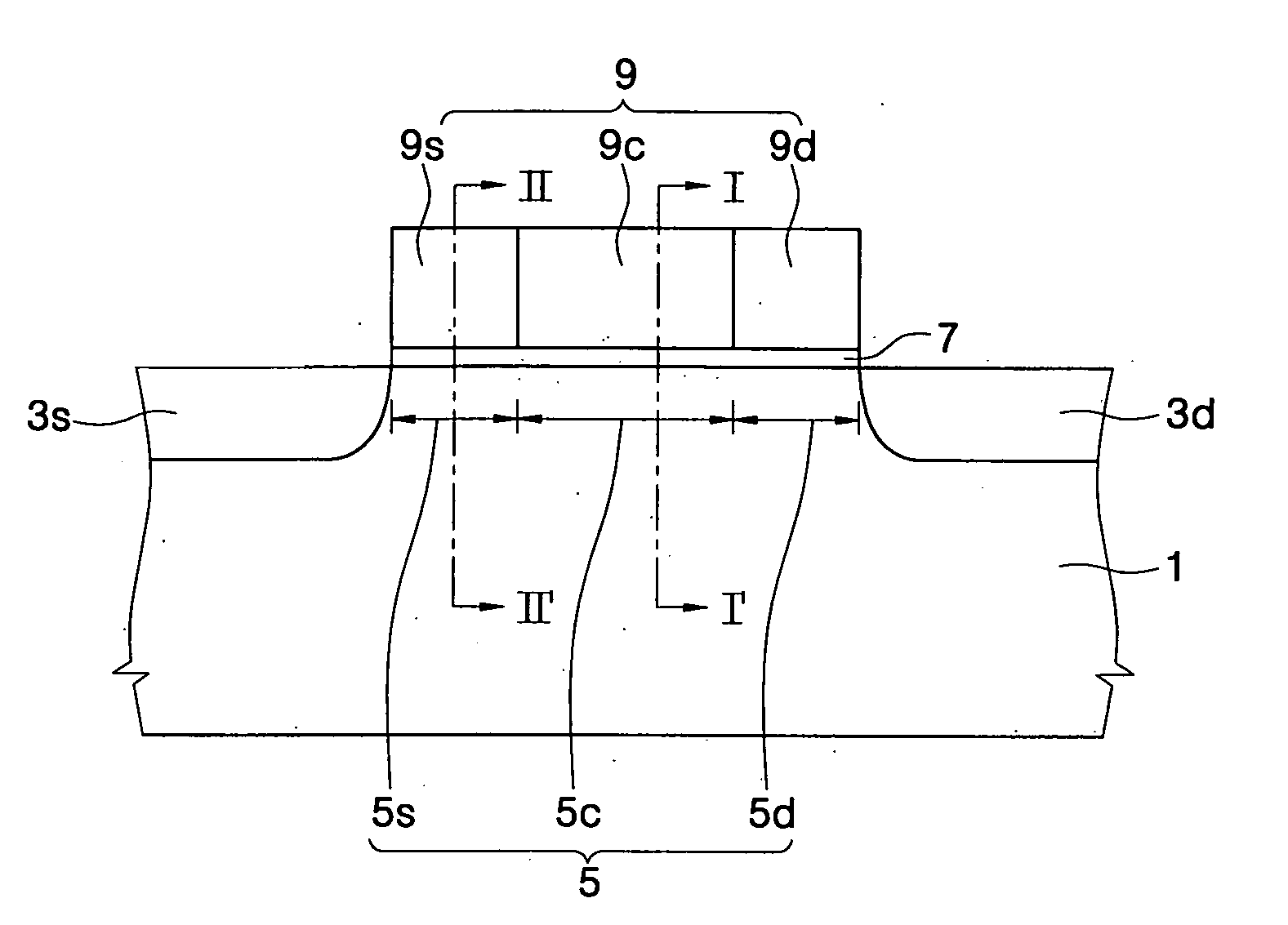
[0011] According to one embodiment of the invention, a metal-oxide semiconductor (MOS) transistor comprises a semiconductor substrate and a central gate electrode formed on the semiconductor substrate, wherein the central gate electrode comprises metal nitride. The transistor further comprises a source side gate electrode and a drain side gate electrode formed on opposite sidewalls of the central gate electrode, wherein the source and drain side gate electrodes comprise doped metal nitride containing first impurities having an electronegativity less than that of nitrogen or second impurities having an electronegativity greater than that of nitrogen, and wherein the source and drain side gate electrodes have respective work functions which are different from a work function of the central gate electrode. The transistor still further comprises a source region formed in the semiconductor substrate, the source region being formed adjacent to the source side gate electrode and located opposite the drain side gate electrode, and, a drain region formed in the semiconductor substrate, the drain region being disposed adjacent to the drain side gate electrode and located opposite the source side gate electrode.
[0012] According to another embodiment of the invention, a complementary metal-oxide semiconductor (CMOS) integrated circuit device comprises a semiconductor substrate having a first region and a second region, a first source region and a first drain region formed in the first region, and a first channel region formed between the first source region and the first drain region. The device further comprises a first metal nitride gate electrode formed on the first channel region, the first metal nitride gate electrode including a first source side gate electrode formed adjacent to the first source region, a first drain side gate electrode formed adjacent to the first drain region, and a first central gate electrode formed between the first source side gate electrode and the first drain side gate electrode. The first source side gate electrode and the first drain side gate electrode typically contain first impurities having an electronegativity less than that of nitrogen and a work function greater than that of the first central gate electrode. The device still further comprises a second source region and a second drain region formed in the second region, and a second channel region formed between the second source region and the second drain region, and a second metal nitride gate electrode formed on the second channel region, the second metal nitride gate electrode including a second source side gate electrode formed adjacent to the second source region, a second drain side gate electrode formed adjacent to the second drain region, and a second central gate electrode formed between the second source side gate electrode and the second drain side gate electrode, wherein the second source side gate electrode and the second drain side gate electrode contain second impurities having an electronegativity greater than that of nitrogen and a work function less than that of the second central gate electrode.
[0013] According to still another embodiment of the invention, a complementary metal-oxide semiconductor (CMOS) integrated circuit device comprises a semiconductor substrate having a first region and a second region, and a first fin body protruding upward from the semiconductor substrate and formed in the first region. The device further comprises a first source region and a first drain region formed in the first fin body and a first channel region formed in the first fin body between the first source region and the first drain region, and a first metal nitride gate electrode formed to cover opposite sidewalls and a top surface of the first channel region, the first metal nitride gate electrode including a first source side gate electrode adjacent to the first source region, a first drain side gate electrode adjacent to the first drain region, and a first central gate electrode between the first source side gate electrode and the first drain side gate electrode, wherein the first source side gate electrode and the first drain side gate electrode contain first impurities having an electronegativity less than that of nitrogen and a work function greater than that of the first central gate electrode. The device still further comprises a second fin body protruding upward from the semiconductor substrate and formed in the second region, and a second source region and a second drain region formed in the second fin body, and a second channel region formed in the second fin body between the second source region and the second drain region. The device still further comprises a second metal nitride gate electrode formed to cover opposite sidewalls and a top surface of the second channel region, wherein the second metal nitride gate electrode comprises a second source side gate electrode adjacent to the second source region, a second drain side gate electrode adjacent to the second drain region, and a second central gate electrode between the second source side gate electrode and the second drain side gate electrode. The second source side gate electrode and the second drain side gate electrode contain second impurities having an electronegativity greater than that of nitrogen and a work function less than that of the second central gate electrode.
[0014] According to still another embodiment of the present inventi

Problems solved by technology

Unfortunately, as the channel length of MOS transistors decreases, the MOS transistors become increasingly susceptible to the short channel effect, which can significantly impair the performance of the semiconductor devices.
Unfortunately, where the halo ion implantation technique is used to fabricate short channel MOS transistors, current drivability of the short channel MOS transistors may be degraded.
This is because the halo ion implantation technique leads to an increase in the impurity concentration of opposing edges of the channel region.
The anisotropic etching steps may cause severe etching da

Method used


Image

  • MOS transistor including multi-work function metal nitride gate electrode, COMS integrated circuit device including same, and related methods of manufacture
  • MOS transistor including multi-work function metal nitride gate electrode, COMS integrated circuit device including same, and related methods of manufacture
  • MOS transistor including multi-work function metal nitride gate electrode, COMS integrated circuit device including same, and related methods of manufacture

Examples


Embodiment Construction

[0029] Exemplary embodiments of the invention are described below with reference to the corresponding drawings. These embodiments are presented as teaching examples. The actual scope of the invention is defined by the claims that follow.

[0030]FIG. 1 is a cross-sectional view illustrating a typical MOS transistor having a multi-work function gate electrode.

[0031] Referring to FIG. 1, a source region 3s and a drain region 3d are formed in a semiconductor substrate 1. A channel region 5 is formed in a region of semiconductor substrate 1 between source region 3s and drain region 3d. A gate electrode 9 is formed on channel region 5, and a gate insulation layer 7 is formed between gate electrode 9 and channel region 5. Gate electrode 9 comprises a source side gate electrode 9s adjacent to source region 3s and a drain side gate electrode 9d adjacent to the drain region 3d as well as a central gate electrode 9c between source side gate electrode 9s and drain side gate electrode 9d. Channe...


PUM


Abstract

Disclosed is a MOS transistor including a multi-work function metal nitride gate electrode. The MOS transistor comprises a semiconductor substrate and a central gate electrode formed on the semiconductor substrate. The central gate electrode is formed of a metal nitride layer. A source side gate electrode and a drain side gate electrode are formed on respective opposite sidewalls of the central gate electrode. The source and drain side gate electrodes are composed of doped metal nitride containing first impurities having an electronegativity less than that of nitrogen or second impurities having an electronegativity greater than that of nitrogen.

Description

BACKGROUND OF THE INVENTION [0001] 1. Field of the Invention [0002] The present invention relates generally to a metal-oxide semiconductor (MOS) transistor and related methods of manufacture. More particularly, the present invention relates to a MOS transistor including a multi-work function metal nitride gate electrode, a complementary metal-oxide semiconductor (CMOS) integrated circuit device including the same, and related methods of manufacture. [0003] A claim of priority is made to Korean Patent Application No. 10-2005-0036416, filed on Apr. 29, 2005, the disclosure of which is hereby incorporated by reference in its entirety. [0004] 2. Description of Related Art [0005] Modern semiconductor devices typically include large numbers of active devices such as MOS transistors. As the level of integration in the semiconductor devices increases, the size of the MOS transistors tends to decrease accordingly. As a result, the channel length of MOS transistors tends to be reduced. Unfort...

Claims


Application Information

Patent Timeline
IPC IPC(8): H01L29/76
CPCH01L21/845H01L27/1211H01L29/785H01L29/4908H01L29/41791H01L21/28088H01L21/28105H01L29/4966
Inventor WANG, XIAOQUANMAEDA, SHIGENOBUKIM, MIN-JOO
Owner SAMSUNG ELECTRONICS CO LTD
Why Eureka
Try Eureka