
Solid-state image pick-up device

a solid-state image and pick-up device technology, applied in the field of solid-state image pick-up devices, can solve the problems of low s/n ratio and long time-consuming for reading out images, and achieve the effect of high s/n ratio

Inactive Publication Date: 2006-11-02
PANASONIC CORP
View PDF8 Cites 20 Cited by
  • Summary
  • Abstract
  • Description
  • Claims
  • Application Information

AI Technical Summary

Benefits of technology

[0010] Therefore, an object of the present invention is to provide a MOS solid-state image pick-up device which is capable of attaining a high S / N ratio.
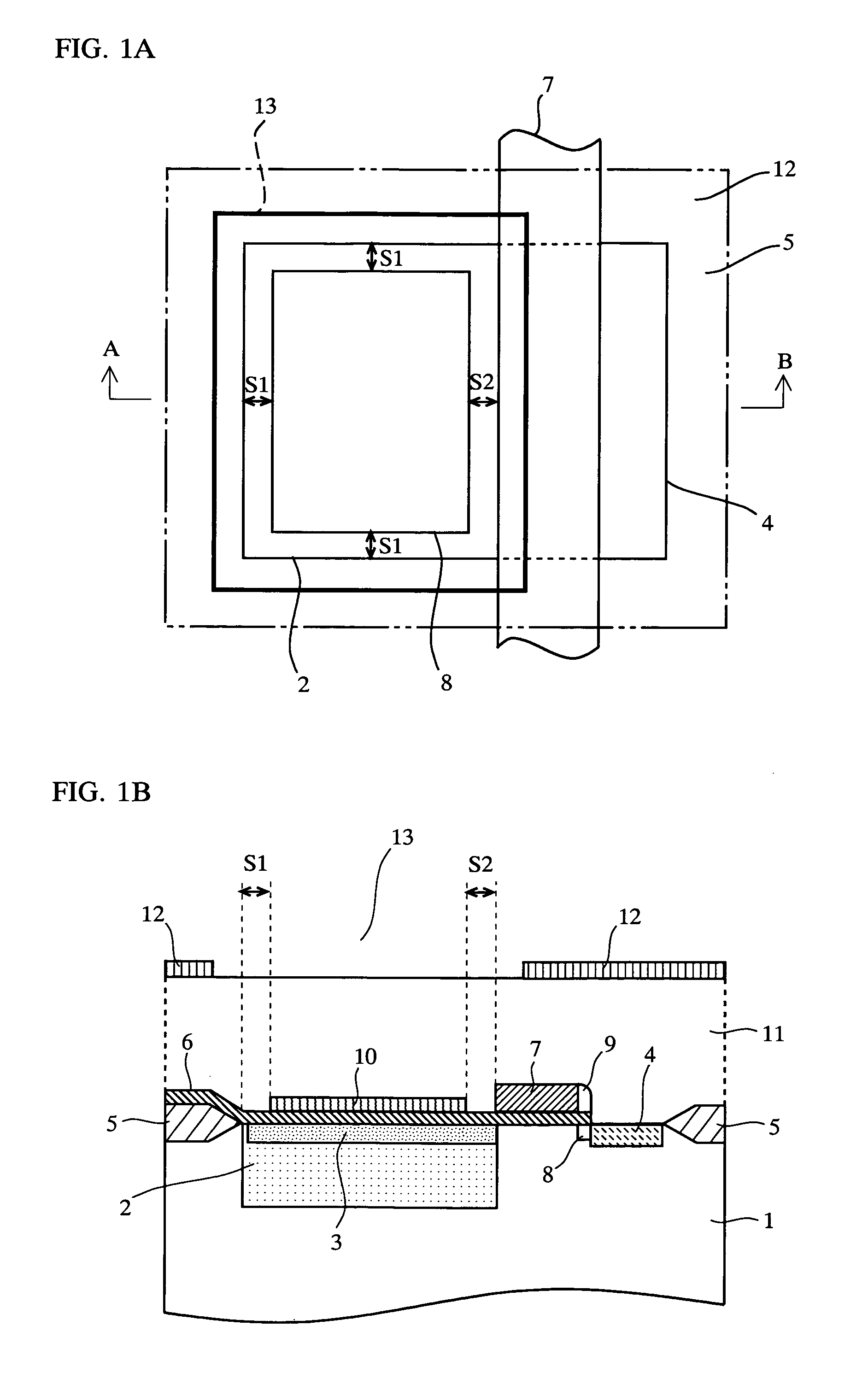
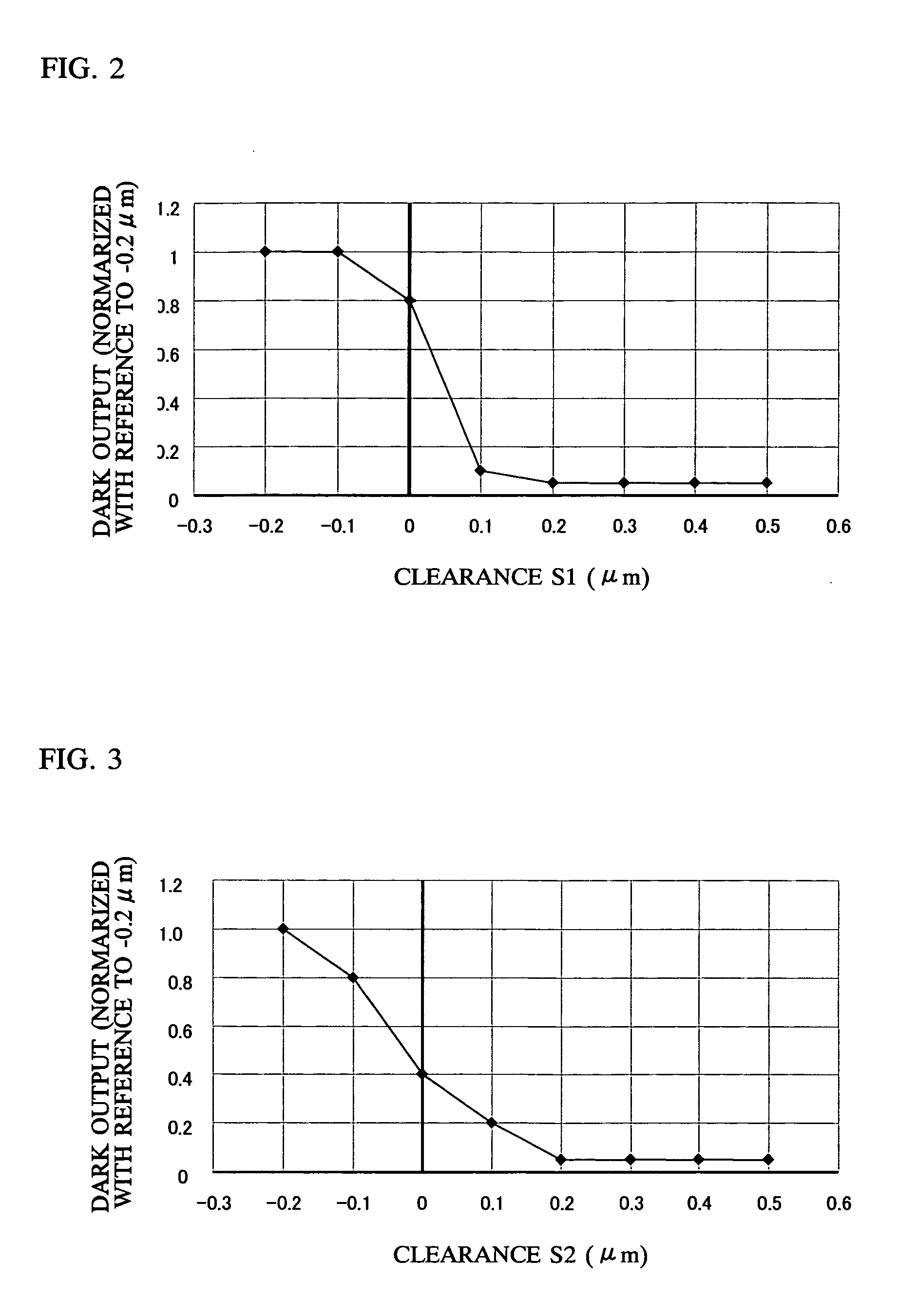
[0015] In the solid-state image pick-up device according to the present invention, the antireflection film is formed not around boundaries between the photo-detecting section and the gate electrode and not around boundaries between the photo-detecting section and the element isolation region, and has a smaller area than the surface area of the photo-detecting section. Through forming the antireflection film in the above-mentioned manner, an increase in a number of surface defects of the semiconductor substrate can be suppressed and thereby an increase in dark output can also be suppressed.
[0016] A microlens is, in general, provided above a photo-detecting region and light collected by a collective lens is collected into the photo-detecting region in a pinpointed manner. Therefore, providing the antireflection film only at a position where light collected by the microlens enters can prevent a reduction in a quantity of light received, as compared with a case where the antireflection film is provided on an entire surface of the photo-detecting region. Therefore, the solid-state image pick-up device according to the present invention can attain high sensitivity, low dark output, and a high S / N ratio.
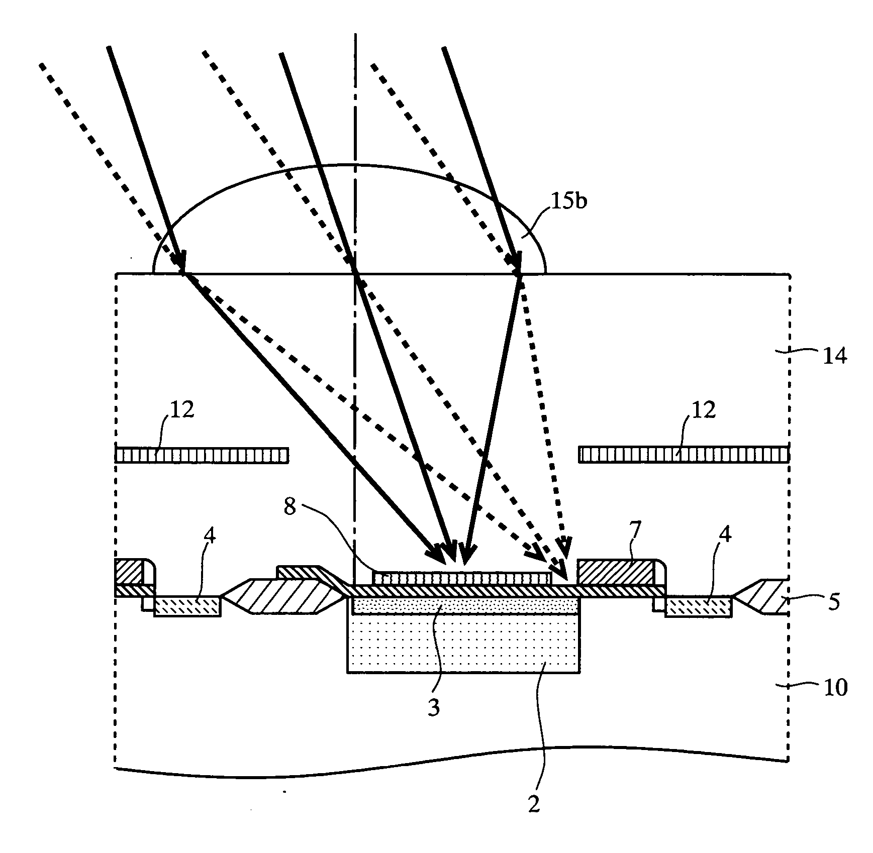
[0017] In addition, if the area of the antireflection film is equal to or greater than 70% of the surface area of the photo-detecting region, a fluctuation in sensitivity among pixels, which may occur when the solid-state image pick-up device is used for a camera with interchangeable lenses, can be suppressed, thus realizing high image quality.

Problems solved by technology

However, the CCD solid-state image pick-up device has a disadvantage of taking a long time for reading out an image signal due to a structure thereof in which a signal electric charge accumulated in a photo-detecting section of a pixel is transferred to a final output section by means of a vertical CCD and a horizontal CCD in a sequential manner and thereafter converted to an electrical signal.
For manufacturing the conventional MOS solid-state image pick-up device, however, since a CMOS logic process is used without any modification, adequate measures for improving sensitivity and reducing the dark output are not taken, resulting in a low S / N ratio.
Accordingly, a challenge in the manufacturing the MOS solid-state image pick-up device is to improve the S / N ratio.

Method used


Image

  • Solid-state image pick-up device
  • Solid-state image pick-up device
  • Solid-state image pick-up device

Examples


first embodiment

[0031]FIG. 1A and FIG. 1B show a top view and a cross-sectional view along a line A-B in FIG. 1A, of a pixel section in a MOS solid-state image pick-up device according to a first embodiment of the present invention. The pixel section, within a semiconductor substrate 1 which is a P-type silicon substrate, comprises an N−-type photo-detecting section 2, a P++-type surface layer 3, an N+-type drain region 4, an isolation region 5, and an N-type LDD (Light Doped Drain) section 8. On a surface of the semiconductor substrate 1, an insulating film 6 which is a silicon oxide film is formed. On the insulating film 6, an antireflection film 10, a gate electrode 7, a side wall 9 of a silicon oxide, an interlayer dielectric film 11, a light-shielding film 12 and the like are formed. An area of the antireflection film 10 is smaller than a surface area of the photo-detecting section 2. An area enclosed by a thick line shown in FIG. 1A is an opening of the light-shielding film 12. An area of the...

second embodiment

[0047] A solid-state image pick-up device according to a second embodiment of the present invention, which comprises an antireflection film 10 having a size suited for use in a camera with interchangeable lenses will be described. The solid-state image pick-up device according to the present embodiment is of a same structure as that of the solid-state image pick-up device which is described in the first embodiment and shown in FIG. 1A and FIG. 1B. The solid-state image pick-up device of the second embodiment is different from the solid-state image pick-up device of the first embodiment in that an area of the antireflection film 10 is equal to or greater than 70% of a surface area of a photo-detecting section 2.

[0048]FIG. 4 is a diagram illustrating a pixel section which comprises microlenses 15a and 15b and photo-detecting sections 2a and 2b, and a camera lens 20. In FIG. 4, pixel sections at positions A and B are, among pixel sections which are disposed in a matrix manner in a pix...


PUM


Abstract

A MOS solid-state image pick-up device with a high S / N ratio is provided. On a surface of a photo-detecting section 2 formed inside a semiconductor substrate, an antireflection film 10 having a smaller area than a surface area of the photo-detecting section 2, with an insulating film 6 imposed therebetween, is provided. The antireflection film 10 is formed so as not to cover bordering portions between the photo-detecting section 2 and peripheral regions thereof. Each of a distance of a clearance S1 between the antireflection film 10 and a gate electrode 7 and a distance of a clearance between the antireflection film 10 and an element isolation region 5 is preferably equal to or greater than 0.2 μm. When the area of the antireflection film 10 is equal to or greater than 70% of the surface area of the photo-detecting section 2, even if used for a camera with interchangeable lenses, a fluctuation in sensitivity among pixels can be suppressed.

Description

BACKGROUND OF THE INVENTION [0001] 1. Field of the Invention [0002] The present invention relates to a MOS solid-state image pick-up device. [0003] 2. Description of the Background Art [0004] Conventionally, as a solid-state image pick-up device, a CCD (Charge Coupled Device) solid-state image pick-up device and a MOS solid-state image pick-up device have been known. The CCD solid-state image pick-up device has an advantage of attaining a high S / N ratio because of high sensitivity and low dark output. Owing to this advantage, the CCD solid-state image pick-up device has conventionally dominated camera markets. However, the CCD solid-state image pick-up device has a disadvantage of taking a long time for reading out an image signal due to a structure thereof in which a signal electric charge accumulated in a photo-detecting section of a pixel is transferred to a final output section by means of a vertical CCD and a horizontal CCD in a sequential manner and thereafter converted to an ...

Claims


Application Information

Patent Timeline
Patent Type & Authority Applications(United States)
IPC IPC(8): H01L31/00H01L27/14H01L27/146H04N25/00
CPCH01L27/14603H01L27/1462H01L31/0232H01L27/14627H01L27/14643H01L27/14623H01L27/14605
Inventor INAGAKI, MAKOTOIGAKI, KAZUAKISAEKI, KOSAKU
Owner PANASONIC CORP
Learn More