Light emitting device and electronic apparatus

a technology of light emitting devices and electronic devices, applied in static indicating devices, electroluminescent light sources, instruments, etc., can solve problems such as deformation or initial defects, and achieve the effect of increasing the viewing angl

Inactive Publication Date: 2006-11-02
SEMICON ENERGY LAB CO LTD
View PDF31 Cites 76 Cited by
  • Summary
  • Abstract
  • Description
  • Claims
  • Application Information

AI Technical Summary

Benefits of technology

[0044] As another example, if the brightness of one color element is controlled using a plurality of regions, one of the regions is referred to as one pixel. In the case of an area gray scale where the brightness of each color element is controlled using a plurality of regions and a gray scale is expressed by all the regions, one pixel means one of the regions for controlling brightness. In that case, one color element is constituted by a plurality of pixels. Further, in that case, each pixel may have a different size area that contributes to display. In addition, slightly different signals may be supplied to a plurality of regions for controlling the brightness of one color element, namely, a plurality of pixels constituting one color element, thereby increasing the viewing angle.

Problems solved by technology

In such a light emitting element, degradation with time or an initial defect may occur.

Method used


Image

  • Light emitting device and electronic apparatus
  • Light emitting device and electronic apparatus
  • Light emitting device and electronic apparatus

Examples


embodiment mode 1

[0090] Described in this embodiment mode is a structure of a light emitting device having a monitoring light emitting element.

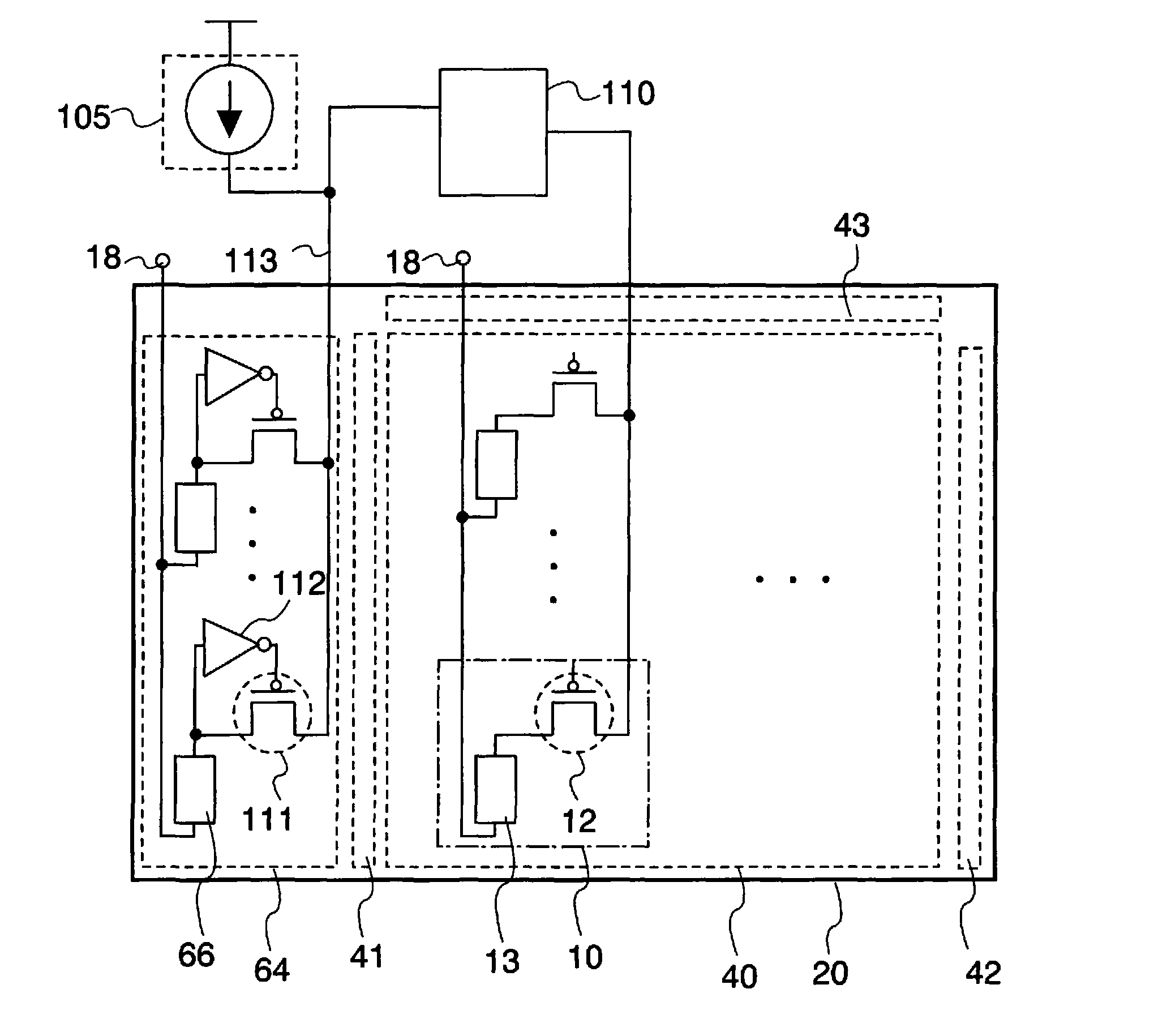
[0091]FIG. 1 shows a pixel portion 40, a signal line driver circuit 43, a first scan line driver circuit 41, a second scan line driver circuit 42, and a monitor circuit 64, which are provided on an insulating substrate 20.

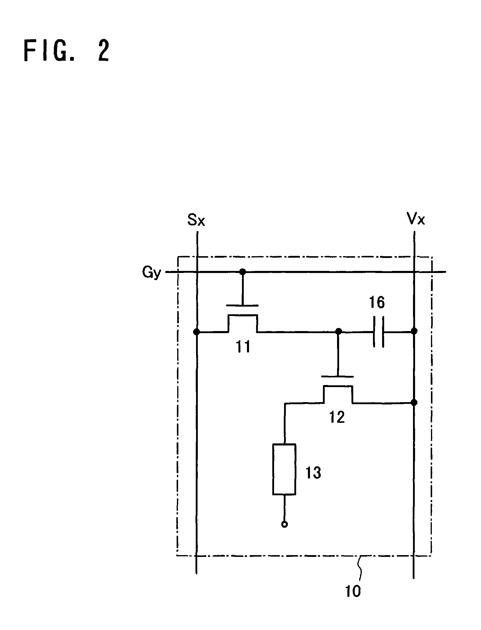
[0092] The pixel portion 40 includes a plurality of pixels 10 each of which has a light emitting element 13 and a transistor (hereinafter referred to as a driving transistor) 12 that is connected to the light emitting element 13 and has a function of controlling current supply. The light emitting element 13 is connected to a power supply 18 denoted by a circle. The structure of the pixel 10 is more specifically described in the following embodiment mode.

[0093] The monitor circuit 64 includes a monitoring light emitting element 66, a transistor (hereinafter referred to as a monitor controlling transistor) 111 connected to the monitoring li...

embodiment mode 2

[0133] Described in this embodiment mode are configuration and operation of a circuit for turning a monitor controlling transistor off when a monitoring light emitting element is short-circuited, which is different from the circuit described in the aforementioned embodiment mode.

[0134] The monitor circuit 64 shown in FIG. 6A includes a first P-channel transistor 80, a second N-channel transistor 81 that has a gate electrode in common with the first transistor and is connected in parallel to the first transistor, and a third N-channel transistor 82 that is connected in series to the second transistor. The monitoring light emitting element 66 is connected to the gate electrode of the first and second transistors 80 and 81. The gate electrode of the monitor controlling transistor 111 is connected to an electrode at which the first and second transistors 80 and 81 are connected to each other. Other configurations are similar to those of the monitor circuit 64 shown in FIGS. 5A and 5B. ...

embodiment mode 3

[0143] In the invention, a reverse bias voltage can be applied to a light emitting element and a monitoring light emitting element. Described in this embodiment mode is the case where a reverse bias voltage is applied.

[0144] If it is assumed that a forward bias voltage is a voltage applied when the light emitting element 13 and the monitoring light emitting element 66 emit light, a reverse bias voltage means a voltage obtained by inverting a High potential and a Low potential of the forward bias voltage. When specifically described using the monitoring light emitting element 66, a potential lower than that of the power supply 18 is applied to the monitor line 113 so that the potentials of the anode electrode 66a and the cathode electrode 66c are inverted.

[0145] Specifically, as shown in FIG. 16, the potential of the anode electrode 66a (anode potential: Va) and the potential of the cathode electrode 66c (cathode potential: Vc) are inverted. At this time, the potential (Vi13) of th...


PUM


Abstract

To solve degradation with time of a light emitting element by a new method. When the potential of an electrode of a monitor pixel is sampled and fed back to a light emitting pixel, degradation with time of a light emitting element can be corrected. In addition, when a writing period is divided into a plurality of periods during which a plurality of rows are selected, a gray scale can be expressed by a weighted light emitting period. That is to say, a light emitting device of the invention has a plurality of monitoring light emitting elements, a monitor line for monitoring changes in the potentials of electrodes of the plurality of light emitting elements, and a means for preventing, when any one of the plurality of monitoring light emitting elements is short-circuited, a current from flowing to the short-circuited monitoring light emitting element through the monitor line.

Description

BACKGROUND OF THE INVENTION [0001] 1. Field of the Invention [0002] The present invention relates to a light emitting device having a self-light emitting element, and a driving method thereof. The invention also relates to an electronic apparatus having a light emitting device including a self-light emitting element. [0003] 2. Description of the Related Art [0004] In recent years, a light emitting device having a light emitting element typified by an EL (Electro Luminescence) element has been developed, and it is expected to be widely used by taking advantages of the self-light emitting type, such as high image quality, wide viewing angle, thin thickness, and lightweight. [0005] In such a light emitting element, degradation with time or an initial defect may occur. In order to prevent degradation with time and an initial defect, suggested is a method where the surface of an anode is swabbed by a PVA (polyvinyl alcohol)-based porous body or the like so as to be planarized and remove ...

Claims


Application Information

Patent Timeline
Patent Type & Authority Applications(United States)
IPC IPC(8): G09G3/32H05B44/00
CPCG09G3/3233G09G2300/0819G09G2320/045G09G2320/043G09G2320/029
Inventor YAMAZAKI, SHUNPEI
Owner SEMICON ENERGY LAB CO LTD
Why Eureka
Try Eureka