Active matrix type display device and driving method thereof

a display device and active matrix technology, applied in the direction of electric digital data processing, instruments, computing, etc., can solve the problems of reducing the display quality, and reducing the time for supplying the voltage to the pixel electrode within b>, so as to improve the driving capability and improve the driving quality of the gray scale signal voltage, without affecting the display quality of the display devi

Active Publication Date: 2006-11-02
RENESAS ELECTRONICS CORP
View PDF6 Cites 50 Cited by
  • Summary
  • Abstract
  • Description
  • Claims
  • Application Information

AI Technical Summary

Benefits of technology

[0080] Accordingly, it is an object of the present invention to improve an active matrix type display device and a driving method therefor, and a column driver of the display device of which driving capability of a gray scale signal voltage is improved and display quality is high, without increasing driving capability of an output buffer, for an increase in a data line impedance (or a resistance of wiring and a capacitance of the wiring) caused by a larger screen of the display device and a higher resolution of the display device.
[0137] According to the present invention, by each of the output switch circuits provided between the output terminals of the buffer amplifiers (operational amplifiers) of the column driver and the one ends of the data lines, supply of the voltage to the corresponding one of the data lines is shut down for the predetermined period until the output signal of the corresponding one of the buffer amplifiers changes to a target gray scale signal voltage corresponding to the video data. Then, after the predetermined period, supply of the voltage to the data line using the output signal of the buffer amplifier is started. Further, a phase of the scan signal is delayed by the predetermined period. With this arrangement, immediately after a period in which the scan signal is set HIGH and the signal voltage of the data line is supplied to the corresponding one of the pixel electrodes has been started, a voltage on the near end of the data line can be instantaneously changed to the target gray scale signal voltage. The supply of the voltage to the data line from the buffer amplifier is stopped before completion of the period in which the signal voltage of the data line is supplied to the pixel electrode. However, by supplying the electric charges held on the data line with a large capacitance to the pixel electrode, the voltage of the pixel electrode can be adequately made close to the target gray signal voltage. The display panel can be thereby driven without degrading display quality thereof.
[0138] According to the present invention, driving capability of the gray scale signal voltage can be improved without increasing driving capability of the buffer amplifier (operational amplifier).
[0139] Further, compared with a display device in which by increasing current consumption of the buffer amplifier (operational amplifier) and enhancing the driving capability of the buffer amplifier, the driving capability of the gray scale signal voltage is improved, the present invention can implement lower power consumption.

Problems solved by technology

Accordingly, 1H is reduced due to the higher definition, and it becomes difficult to secure a time for supplying the voltage to the pixel electrodes within 1H (time TC in FIG. 13).
As a result, the gray scale signal voltage to be supplied to the pixel electrodes does not adequately reach the target voltage, so that the display quality degrades.

Method used


Image

  • Active matrix type display device and driving method thereof
  • Active matrix type display device and driving method thereof
  • Active matrix type display device and driving method thereof

Examples


first embodiment

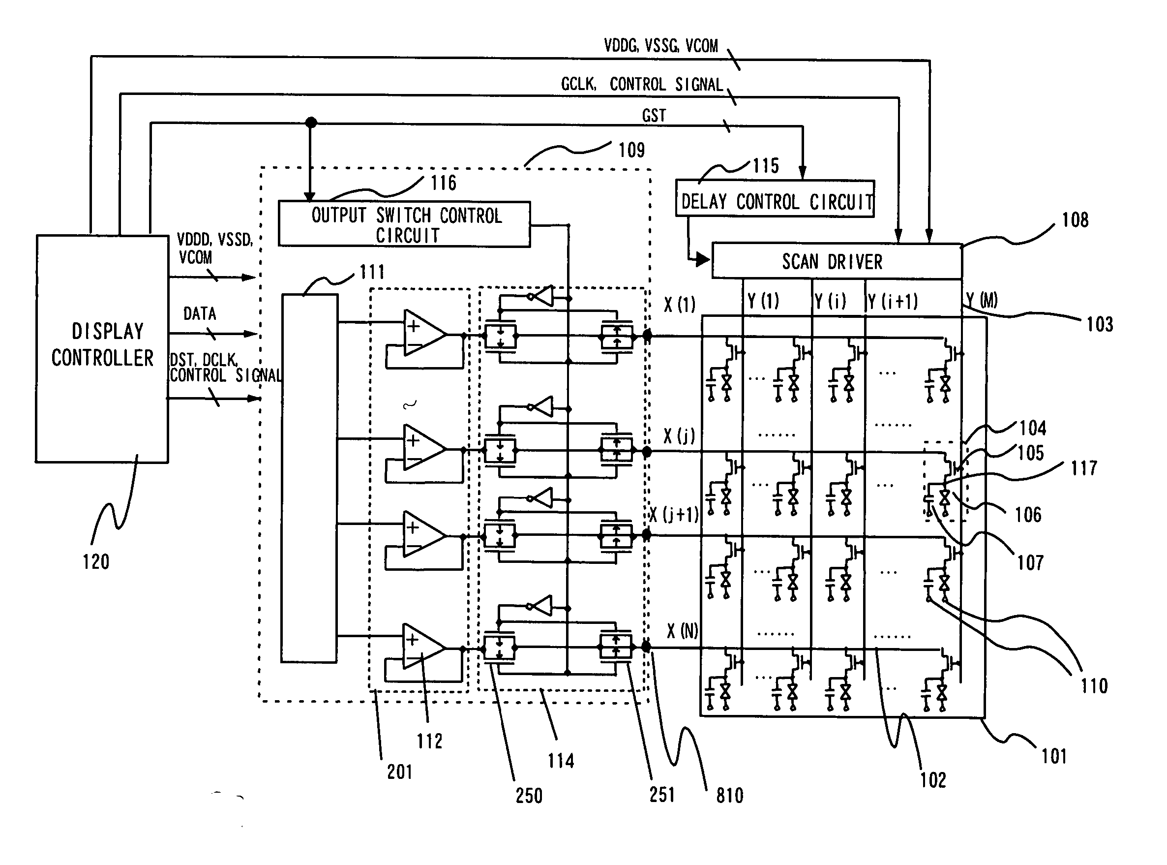
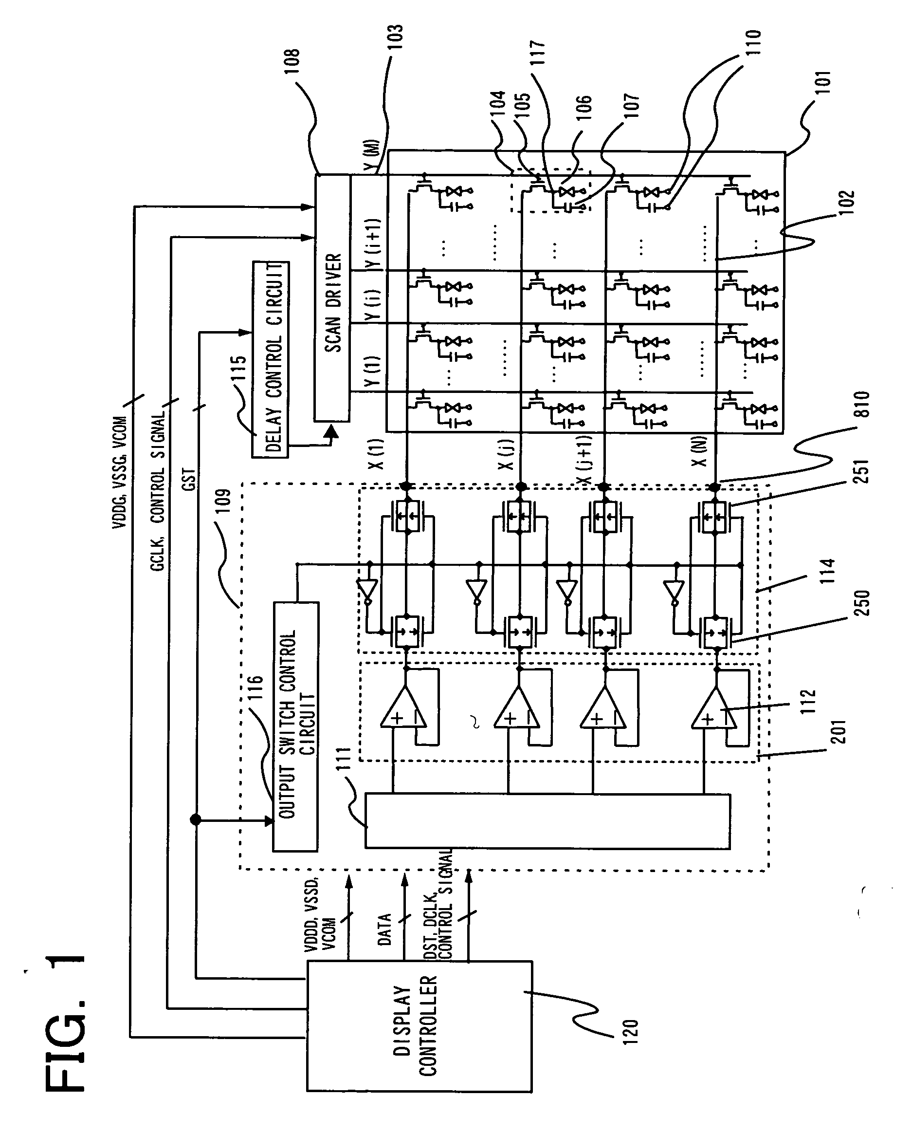
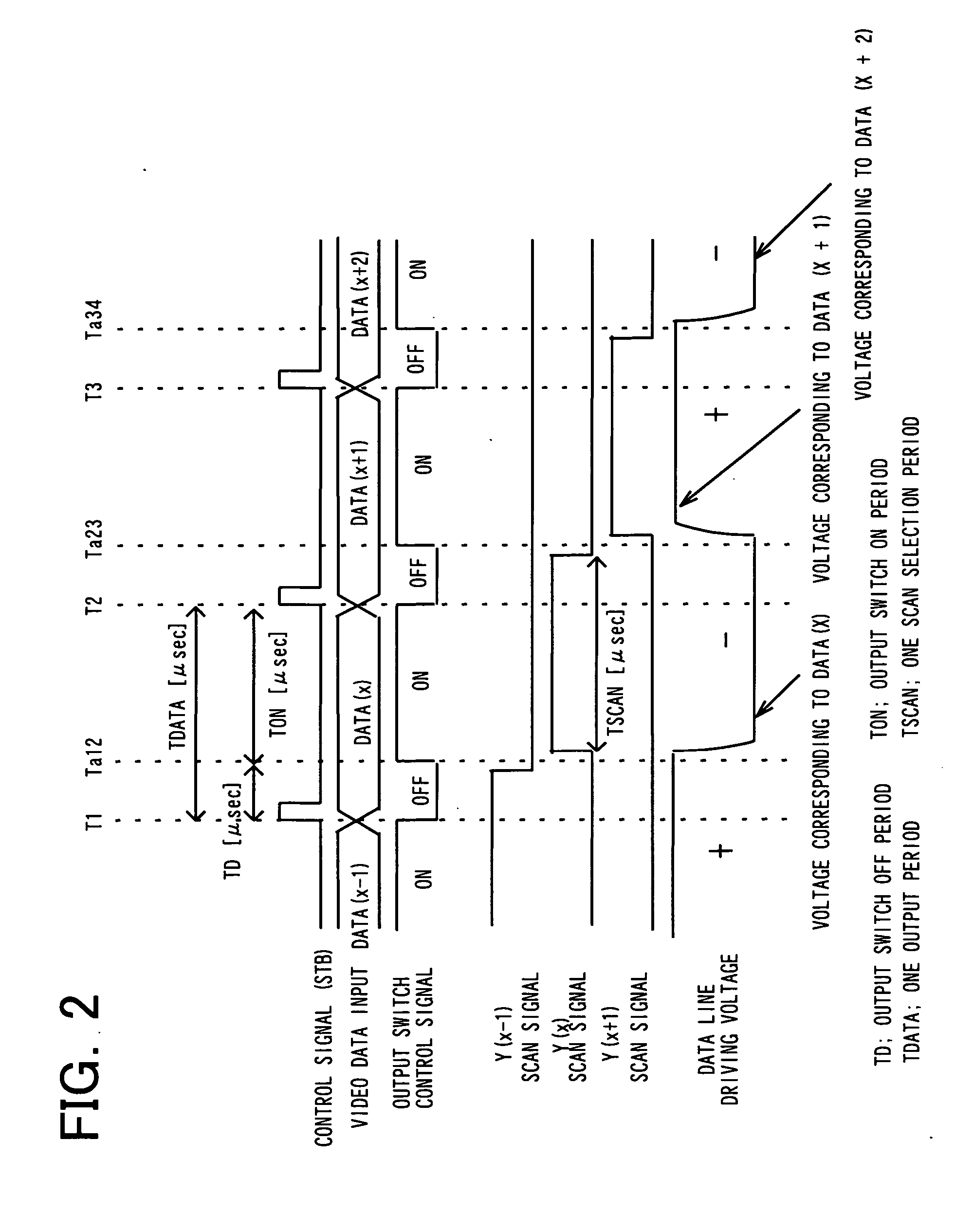
[0161] A configuration of a first embodiment of the present invention will be described below. FIG. 1 is a diagram showing a configuration of an active matrix type liquid crystal display device according to the first embodiment of the present invention. Referring to FIG. 1, the active matrix type liquid crystal display device of the present invention includes a liquid crystal panel 101, a scan driver 108, a column driver 109, a display controller 120, a delay control circuit 115, and an output switch control circuit 116.

[0162] The liquid crystal panel 101 is constituted from two substrates and a liquid crystal sandwiched between these two substrates. One of the substrates includes scan lines 103, data lines 102, and pixel circuits 104 provided at intersections between the scan lines 103 and the data lines 102. For each pixel, a pixel circuit 104 is formed.

[0163] Output terminals of the scan driver 108 are connected to one ends of the scan lines 103, and output terminals of the col...

second embodiment

[0224] A second embodiment of the present invention will be described below. FIG. 3 is a diagram showing a configuration of an active matrix type liquid crystal display device according to the second embodiment of the present invention. This embodiment is different from the first embodiment shown in FIG. 1 in the buffer amplifiers 201, output switch circuits 114, and preceding-stage circuit unit 111. Other configurations are the same as those in the first embodiment. A difference from the first embodiment will be described below.

[0225] Each of the buffer amplifiers 201 has a configuration in which a positive output side operational amplifier 901 and a negative output side operation amplifier 902 are alternately arranged, and respectively provided for each data line.

[0226] The positive output side operational amplifier 901 is the operational amplifier that outputs a positive voltage with respect to a voltage Vcom of the common electrode 110 for the liquid crystal panel 101. The neg...

third embodiment

[0255] A configuration of a third embodiment of the present invention will be described below. FIG. 5 is a diagram showing a configuration of an active matrix type liquid crystal display device according to the third embodiment of the present invention. Referring to FIG. 5, a difference between the present embodiment and the first embodiment described before, shown in FIG. 1 is that an operational amplifier having an offset cancelling function is used for each of the buffer amplifiers 201.

[0256] As the operational amplifier having the offset canceling function used in the configuration shown in FIG. 5, a configuration as shown in FIG. 7, for example, is employed. FIG. 7 is a diagram showing the configuration of an operational amplifier disclosed in Patent Document 9 (Japanese Patent Kokai Publication No. JP-A-9-244590). Other configuration can be similarly used, if it is the operational amplifier having the offset cancelling function. Since a configuration of the liquid crystal pan...


PUM


Abstract

Disclosed is a display device including display unit, a column driver, a delay control circuit, an output switch control circuit, and a display controller. The display unit includes a plurality of pixel electrodes arranged at intersections between a plurality of data lines and a plurality of scan lines in a matrix form and TFTs. One of a drain and a source of each of the TFTs is connected to a corresponding one of the pixel electrodes. The other one of the drain and the source of each of the TFTs is connected to a corresponding one of the data lines, and a gate of each of the TFTs is connected to a corresponding one of the scan lines. The scan driver supplies a scan signal to each of the scan line in a preset scan cycle. The column driver includes D / A converter circuits for converting video data to gray scale signals, a plurality of buffer amplifiers for sequentially amplifying and outputting the gray scale signals in a preset output cycle, and an output switch circuit including a plurality of switches connected to output terminals of the buffer amplifiers and the data lines, respectively. The delay control circuit controls the scan driver so that the preset scan cycle is delayed from the preset output cycle just by a preset delay time. The output switch control circuit controls the output switch circuit to be kept off during the preset delay time. The display controller controls the video data, scan driver, column driver, delay control circuit, and output switch control circuit, respectively.

Description

FIELD OF THE INVENTION [0001] The present invention relates to an active matrix type display device and a driving method thereof. More specifically, the invention relates to a display device including circuit means suitable for driving a data line with a large-capacitance load and a driving method thereof. BACKGROUND OF THE INVENTION [0002] Liquid crystal display devices (LCDs) characterized by their thin design, light weight and low power consumption have come into widespread use in recent years and are utilized in the display units of mobile devices such as portable telephones (mobile telephones or cellular telephones), PDAs (Personal Digital Assistants) and laptop personal computers. A system for driving these liquid crystal display devices is classified into a simple matrix type and an active matrix type. It is the active matrix type that is suitable for achieving higher definition. The active matrix type display device has a switching device for each pixel. [0003] Since the act...

Claims


Application Information

Patent Timeline
Patent Type & Authority Applications(United States)
IPC IPC(8): G09G3/36
CPCG09G3/3266G09G3/3275G09G2300/0842G09G2330/021G09G2310/027G09G2320/0252G09G2310/0248
Inventor IRIGUCHI, MASAOTSUCHI, HIROSHI
Owner RENESAS ELECTRONICS CORP
Why Eureka
Try Eureka