Optical element obtained by homeotropically orienting liquid crystal molecule, member for liquid crystal display device using the same, and liquid crystal display device

a liquid crystal molecule and optical element technology, applied in the direction of optical elements, instruments, transportation and packaging, etc., can solve the problems of significant increase in production cost, limited number of liquid crystal display devices each capable of using liquid crystal film, and damage to orientation, so as to prevent any damage to orientation, reduce the thickness of the liquid crystal display device, and reduce the production cost of the optical element of the present invention

Active Publication Date: 2006-11-02
DAI NIPPON PRINTING CO LTD
View PDF5 Cites 5 Cited by
  • Summary
  • Abstract
  • Description
  • Claims
  • Application Information

AI Technical Summary

Benefits of technology

[0032] In addition, in the present invention, an isotropic layer composed of a non-oriented liquid crystal monomer is formed on the surface of the birefringence layer, so the isotropic layer serves as a protective layer to protect the orientation of a liquid crystal polymer constituting the birefringence layer from an external factor and to prevent any damage to the orientation. Therefore, the present invention has no possibility that damage to orientation due to an external factor reduces the phase difference control function of a birefringence layer.
[0033] The above optical element can be laminated and formed integrally on a member constituting a liquid crystal panel, and an optical instrument can be designed without the separate arrangement of any member (phase difference control member) such as a film for controlling a phase difference. Separately arranging a phase difference control member requires the fixing of the member by means of an adhesive or the like. However, the optical element of the present invention can eliminate the need for such adhesive, and can reduce the possibility of, for example, the scattering of light due to an adhesive.
[0034] When the optical element of the present invention is provided with a coloring layer, and the resultant is used for a liquid crystal display device, the need to arrange a phase difference control member separate from a member having the coloring layer is eliminated, so the thickness of the liquid crystal display device can be reduced.
[0035] The production cost of the optical element of the present invention can be easily suppressed because the birefringence layer can be formed through a relatively easy process involving: applying, to the upper surface of a base material or the upper surface of a vertical alignment layer formed by applying a composition liquid for the upper film of the base material, a birefringence layer composition liquid; orienting liquid crystal; and crosslinking the liquid crystal.
[0036] A member for a liquid crystal display device using the optical element can improve a phase difference control function, and a liquid crystal display device provided with the characteristics of the optical element such as a reduction in possibility of light scattering due to an adhesive can be produced by means of the member.
[0037] In addition, the thickness of a liquid crystal display device using the optical element can be reduced as compared to that of a liquid crystal display device formed by means of a conventional optical compensating film. In addition, the liquid crystal display device can effectively utilize light, has good contrast, and can provide a wide visual angle.

Problems solved by technology

The viewing angle compensation film of JP 05-142531 A has a problem in that a production cost significantly increases because the film is obtained through a large number of production steps as described above.
When a homeotropically oriented liquid crystal layer is obtained by means of the method, there arises a problem in that a production cost significantly increases.
In this case, it is difficult to use a homeotropically oriented liquid crystal film obtained by means of the method for a liquid crystal display device requested to have high heat resistance, so the number of liquid crystal display devices each of which is capable of using the liquid crystal film is limited.
In addition, when a homeotropically oriented liquid crystal film obtained by means of the method is used for a liquid crystal display device, attention must be paid in such a manner that the film is not placed in a high-temperature environment, so it is difficult to arrange the film inside the liquid crystal display device.
Therefore, a homeotropically oriented liquid crystal film obtained by means of the method of JP 2002-174725 A has a problem in that the number of positions where the film can be installed in a liquid crystal cell is limited.

Method used


Image

  • Optical element obtained by homeotropically orienting liquid crystal molecule, member for liquid crystal display device using the same, and liquid crystal display device
  • Optical element obtained by homeotropically orienting liquid crystal molecule, member for liquid crystal display device using the same, and liquid crystal display device
  • Optical element obtained by homeotropically orienting liquid crystal molecule, member for liquid crystal display device using the same, and liquid crystal display device

Examples


example 1

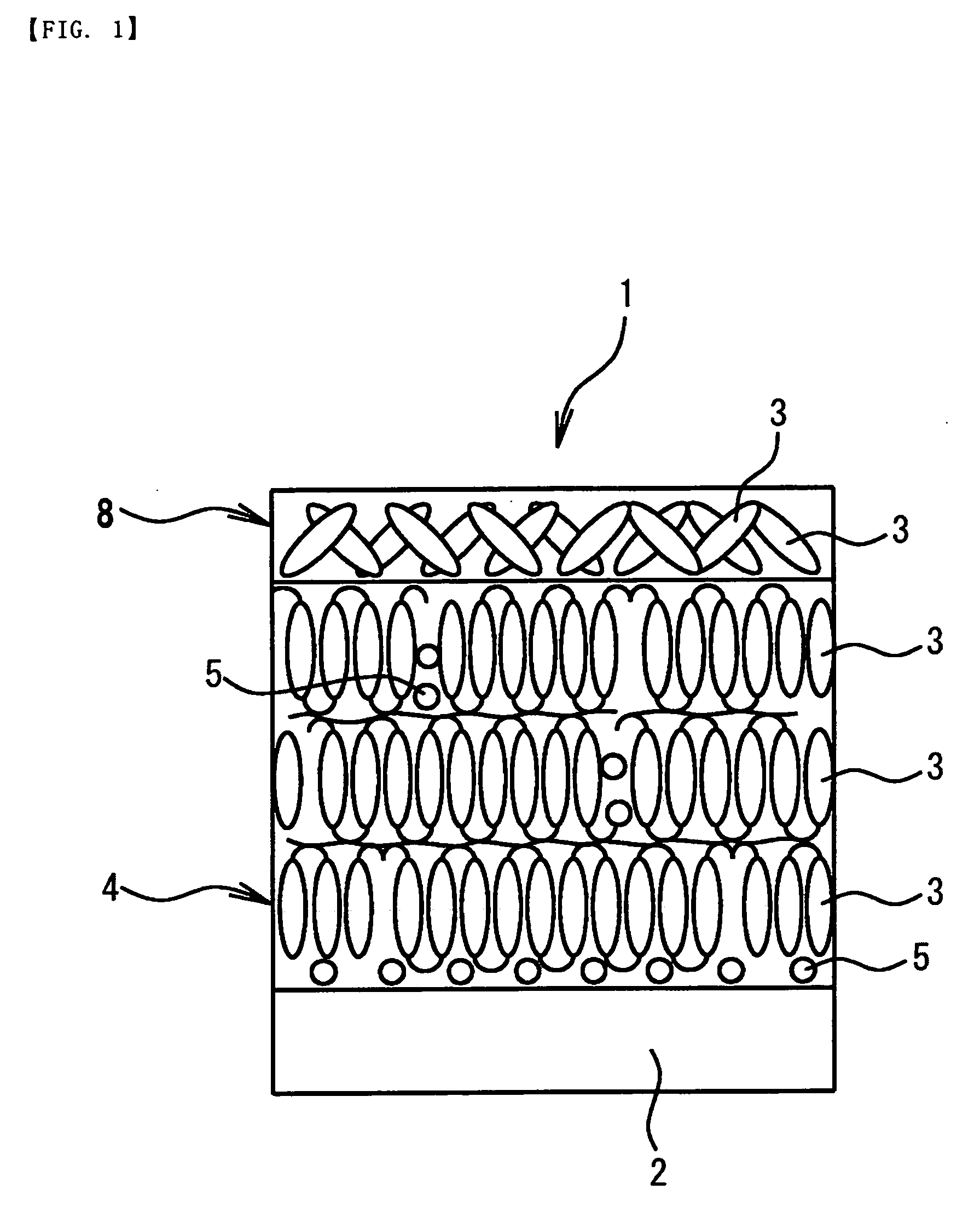
[0193] The vertical alignment layer solution was patterned onto the upper surface of a glass base material by means of a flexographic printing method to form a film having a thickness of 600 Å. The resultant was baked at 180° C. for 1 hour, so a vertical alignment layer was formed on the glass base material. Next, the base material on which the vertical alignment layer had been formed was installed in a spin coater (trade name “1H-360S” manufactured by MIKASA), and the birefringence layer composition liquid prepared in advance was applied to the upper surface of the alignment layer by means of spin coating in such a manner that a thickness after drying would be about 1.5 μm. In this example, a spin coating method was adopted as a method of applying a liquid crystal solution. However, a method of applying a liquid crystal solution is not limited thereto. For example, die coating, slit coating, and an approach as a result of combination of them can be appropriately selected. The same ...

example 2

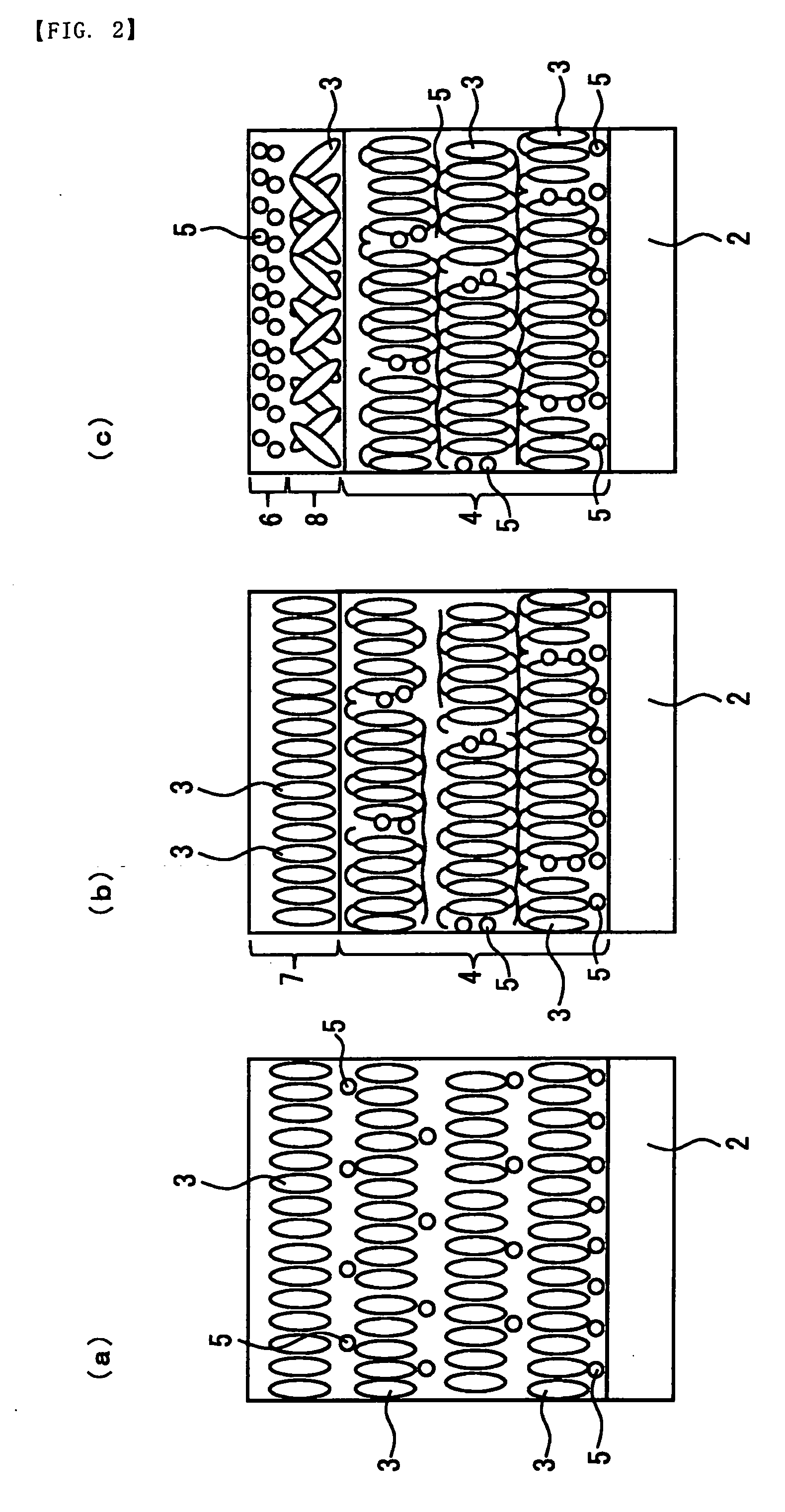
[0197] A base material 2 was formed in the same manner as in Example 1, and Example 2 was produced in the same manner as in Example 1 except that the surface of the base material 2 (surface opposite to the glass base material) was ground by means of a grinding attachment by 1,000 Å.

example 3

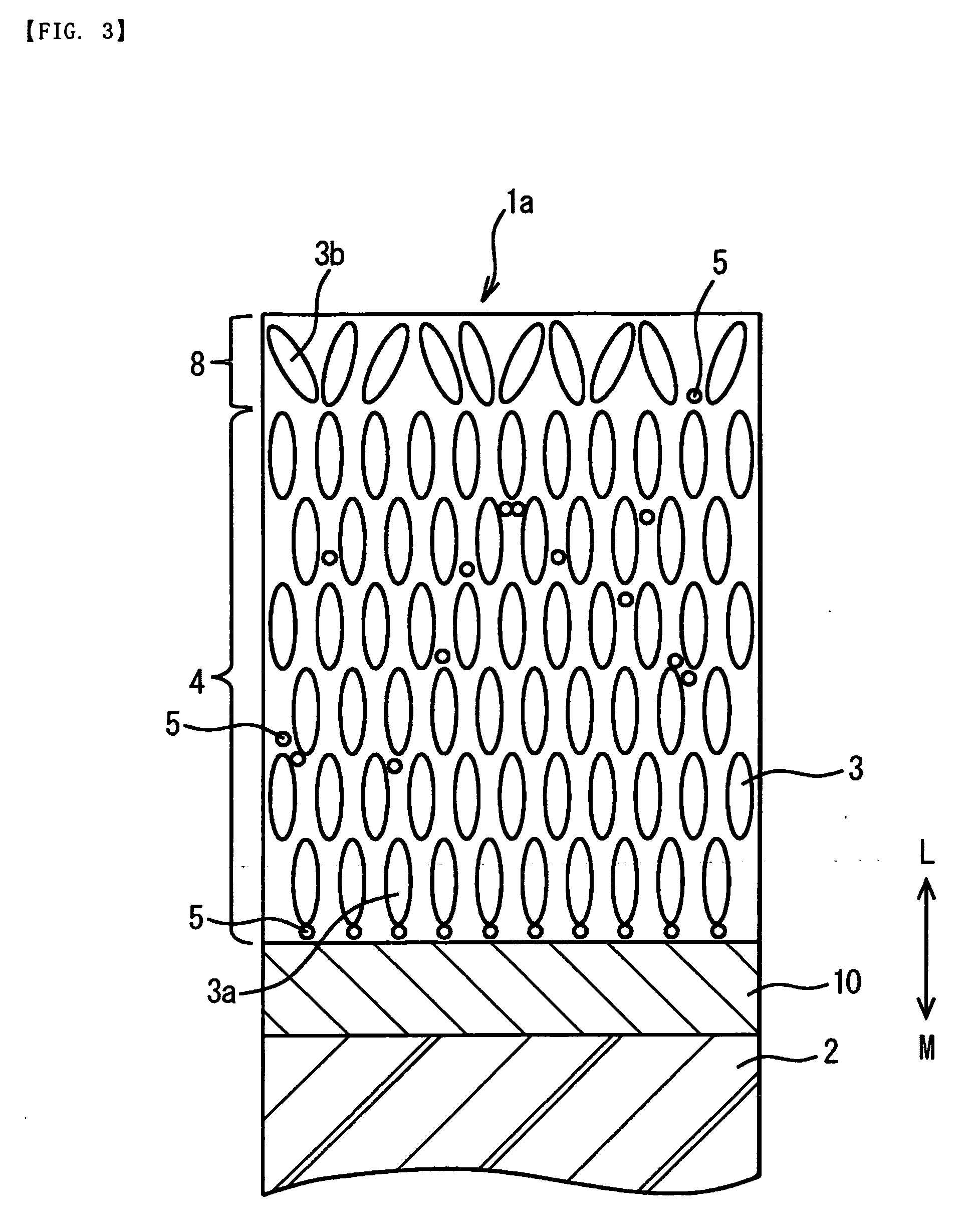
[0209] The liquid crystal display device shown in FIG. 9B was produced as a liquid crystal display device using the optical element of the present invention, and was defined as Example 3.

[0210] The optical element of the present invention was formed in the same manner as in Example 1 except that a coloring layer was formed between a glass base material washed through a pretreatment and a vertical alignment layer in order to produce Example 3.

[0211] To form the above coloring layer, at first, a photoresist for a BM prepared as described above was applied to the upper surface of the glass base material by means of a spin coating method to have a thickness of 1.2 μm, and the whole was pre-baked at 80° C. for 3 minutes. Then, the resultant was exposed to light (100 mJ / cm2) by means of a mask formed into a predetermined pattern. Subsequently, the resultant was subjected to spray development with a 0.05% aqueous solution of KOH for 50 seconds. After that, the resultant was post-baked at...


PUM

PropertyMeasurementUnit
specific gravityaaaaaaaaaa
thicknessaaaaaaaaaa
thicknessaaaaaaaaaa

Abstract

An object of the present invention is to provide an optical element which can suppress a production cost, has good heat resistance; uniformly maintains the fixed orientation of a liquid crystal polymer in a wide temperature range, shows a low haze with reliability without reducing birefringence property owing to a physical factor from its external surface, and can maintain desired birefringence property with reliability. The present invention relates to an optical element formed by forming, on the upper surface of a base material having light permeability, at least a birefringence layer having a structure obtained by fixing liquid crystal monomers each having a polymerizable group at a terminal thereof in a state where the monomers are homeotropically oriented, forming an isotropic layer constituted by the liquid crystal monomers on the upper surface of the birefringence layer, and removing an additive layer formed on the upper surface of the isotropic layer.

Description

BACKGROUND OF THE INVENTION [0001] 1. Field of the Invention [0002] The present invention relates to an optical element having a birefringence functional layer. More specifically, the present invention relates to an optical element having a birefringence functional layer including a birefringence layer obtained by orienting and fixing a liquid crystal molecule, a member for a liquid crystal display device using the optical element, and liquid crystal display device. [0003] 2. Description of the Related Art [0004] A liquid crystal display device has found use in a variety of fields such as a television and medical equipment because the device has such advantages that the thickness and the weight of the device can be readily reduced, power consumption can be reduced, and a flicker hardly occurs. On the other hand, the device involves a problem which causes light leak or a tone reversal phenomenon depending on the angle at which a user views a liquid crystal display screen, that is, a ...

Claims


Application Information

Patent Timeline
Patent Type & Authority Applications(United States)
IPC IPC(8): C09K19/00
CPCC09K19/2007C09K19/322C09K19/3852C09K2019/0448Y10T428/1036G02F1/133634Y10T428/1005Y10T428/10G02B5/3083C09K2323/03C09K2323/02C09K2323/00C09K19/56G02F1/1337
Inventor SUEMASU, ATSUSHI
Owner DAI NIPPON PRINTING CO LTD
Why Eureka
Try Eureka