Method of fabricating a transistor having a triple channel in a memory device

a memory device and triple channel technology, applied in the field of semiconductor devices, can solve the problems of undesirable increase of resistance of low-resistant gate electrodes, limitation of conventional two-dimensional planar channel structures to obtain target threshold voltage, and serious influence of threshold voltage on channel width

Active Publication Date: 2006-11-02
SK HYNIX INC
View PDF10 Cites 15 Cited by
  • Summary
  • Abstract
  • Description
  • Claims
  • Application Information

AI Technical Summary

Benefits of technology

[0029] If the transistor is fabricated through the above process, the predetermined portion of the field oxide layer is selectively etched so as to allow the gate electrode to pass therethrough. Therefore, the first conductive layer to be patterned may have the same th...

Problems solved by technology

As the semiconductor devices are equipped with a short channel structure, the threshold voltage exerts a serious influence on the channel width.
Accordingly, the conventional two-dimensional planar channel structure presents limitations to obtain the target threshold voltage of the transistor required for a specific semiconductor device.
All of these factors contribute to undesirable increase of resistance of the low-resistant gate electrode 4.
If the low-resistant gate electrode 4 is fabricated by depositing an upper layer on a lower layer p...

Method used


Image

  • Method of fabricating a transistor having a triple channel in a memory device
  • Method of fabricating a transistor having a triple channel in a memory device
  • Method of fabricating a transistor having a triple channel in a memory device

Examples


first embodiment

[0050]FIGS. 5A and 5B illustrate the structure of the transistor fabricated by the process according to the present invention, wherein FIG. 5A is a cross-sectional view taken along line A-A′ shown in FIG. 4F, and FIG. 5B is a cross-sectional view taken along line B-B′ shown in FIG. 4F.

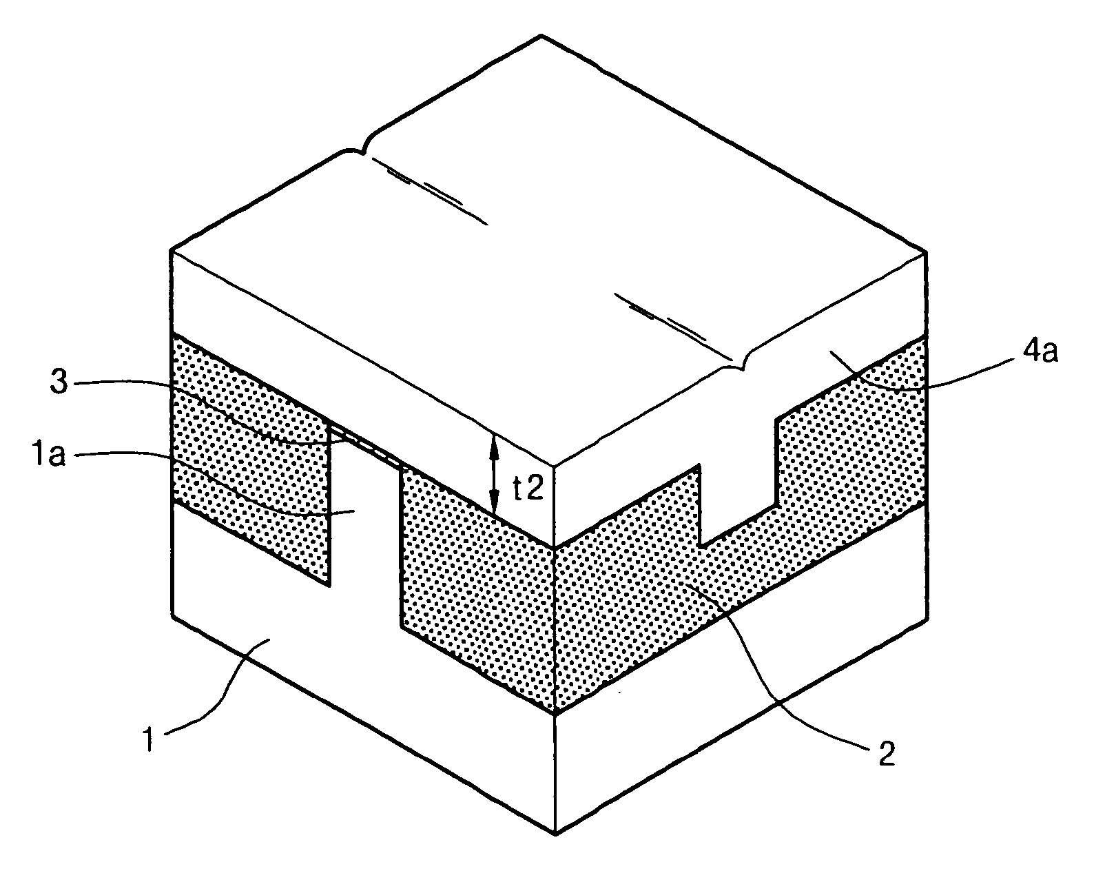
[0051] It can be understood from FIGS. 5A and 5B that the transistor according to the first embodiment of the present invention has the following structure. That is, the transistor includes the active area 1a vertically protruding from the predetermined portion of the semiconductor substrate 1 and the field oxide layer 2 is formed at both sides of the active area 1a. In addition, the recess g integrally formed with the channel area provided in the active area 1a is formed in the field oxide layer 2 in such a manner that the gate electrode passes through the recess g. The low-resistant gate electrode 4, which extends through the upper portion of the active area 1a while being overlapped with the channel...

second embodiment

[0063]FIGS. 7A to 7D illustrate the structure of the transistor fabricated according to the present invention, wherein FIG. 7A is a cross-sectional view taken along line A-A′ shown in FIG. 6G; FIG. 7B is a cross-sectional view taken along line A1-A1′ shown in FIG. 6G; FIG. 7C is a cross-sectional view taken along line B-B′ shown in FIG. 6G; and FIG. 7D is a cross-sectional view taken along line B1-B1′ shown in FIG. 6G.

[0064] It can be understood from FIGS. 7A to 7D that the transistor according to the second embodiment of the present invention has the following structure. That is, the transistor includes the active area 1a vertically protruding from the predetermined portion of the semiconductor substrate 1 and the field oxide layer 2 is formed at both sides of the active area 1a. In addition, the first recess g1 having the depth d1 is formed in channel area of the active area 1a. Accordingly, the height Hc (FIG. 7C) of the channel section of the active area 1a is lower than the hei...


PUM


Abstract

Disclosed is a method for fabricating a transistor of a memory device capable of preventing voids from being created when forming a low-resistant gate electrode. The method includes the steps of forming an active area by etching a semiconductor substrate, forming a field oxide layer in the semiconductor substrate and forming a recess by etching the field oxide layer. A gate insulation layer is formed along an upper surface of the active area and an exposed portion of the active area. A gate electrode is formed on the field oxide layer such that the gate electrode extends across an upper portion of the active area while being overlapped with a channel area and the recess. The first conductive layer to be patterned has the same thickness, so the low-resistant gate electrode is easily fabricated without forming the voids.

Description

BACKGROUND OF THE INVENTION [0001] 1. Field of the Invention [0002] The present invention relates to a method of fabricating a semiconductor device. More particularly, the present invention relates to a method of fabricating a transistor having a triple channel in a memory device. [0003] 2. Description of the Prior Art [0004] Recently, as semiconductor devices have been highly integrated, channel lengths and channel widths of a transistor are significantly shortened. As the semiconductor devices are equipped with a short channel structure, the threshold voltage exerts a serious influence on the channel width. Accordingly, the conventional two-dimensional planar channel structure presents limitations to obtain the target threshold voltage of the transistor required for a specific semiconductor device. [0005] In order to solve the above problem, studies and researches have been actively performed in relation to a three-dimensional transistor for applications in a logic device. In part...

Claims


Application Information

Patent Timeline
IPC IPC(8): H01L21/336H01L21/76
CPCH01L27/105H01L27/10876H01L27/10879H01L27/1052H01L29/66795H01L29/7851H01L29/66621H10B99/00H10B12/056H10B12/053H01L21/18
Inventor JANG, SE AUGKIM, YONG SOOOH, JAE GEUN
Owner SK HYNIX INC
Why Eureka
Try Eureka