Method and system for BitMap Analysis System for high speed testing of memories

Inactive Publication Date: 2006-11-02
STMICROELECTRONICS PVT LTD
View PDF5 Cites 6 Cited by
  • Summary
  • Abstract
  • Description
  • Claims
  • Application Information

AI Technical Summary

Benefits of technology

[0020] The present invention provides a bit map analysis methodology with a unique architecture, which solves the problems created by the above-ment

Problems solved by technology

There are several problems that are commonly encountered while generating the bitmap.
It is observed that more faults occur at high clock speeds for reading/writing from memories.
However, most testers today operate at a very low clock speed as the I/O's for the testers fail at high frequencies.
Due to this problem, many faults that should be detected may be missed.
However, sometimes this information is also big and it takes a lot of space to store it as well as to send it out to the tester.
This is not an effective technique.
This process takes a long time, and extra software and resources are required in the tester to generate a bitmap of the memory.
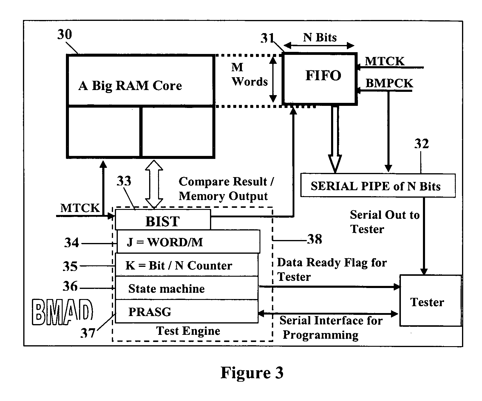
The drawbacks of this method are that no matter how big a FIFO is used, one can never stop the BIST from waiting for the tester to read the complete information once the FIFO stack is full.
Thus, FIFO stack height can never be decided with surety.
In addition, the raw information to be stored is again very big.
Thus, considerable area and time is consumed in this method, and all the efforts of generating a high-speed bit map of the memory are wasted if the stack is full and the BIST has to wait.
The problem with this methodology is that this counter is unused if there are very few faults.
In addition, if there are a large number of faults, then one needs a very big counter.
Also this method needs a lot of time and hard

Method used


Image

  • Method and system for BitMap Analysis System for high speed testing of memories
  • Method and system for BitMap Analysis System for high speed testing of memories
  • Method and system for BitMap Analysis System for high speed testing of memories

Examples


Embodiment Construction

[0033] In the current approach of analyzing memory faults and creating a bitmap, a FIFO is used as an interface between a BIST and a tester. The invention divides a big memory core into many small logical memory cores and generates a bit map for the same that can be stored in a smaller FIFO.

[0034]FIG. 3 shows a block diagram of an embodiment of a Bit Map Analysis System (BMAS) of the invention. It contains a RAM core 30, BIST 33 that contains the March Element Opcode Loader and is linked to RAM core 30, a FIFO 31 with M words and N data bits connected to a Serial Pipe 32 to convert N bits to 1-bit information per tester clock. The embodiment also includes a counter 34 which counts up to (Total Words) / M, a counter 35 which counts up to (Total Data Bits) / N, a state machine 36 to organize all the activities and manage the handshake signals with the tester and a Programmable Read Address Sequence Generator (PRASG) 37 for configuring the address sequence from tester through a serial int...


PUM


Abstract

A Bit Map Analysis System (BMAS) for high-speed memory testing. The BMAS reduces the amount of data transaction between the BIST and tester may be used in embedded memories, whether asynchronous or synchronous, static or dynamic, or volatile or non-volatile. The tester clock cycle is substantially reduced, resulting in reduced diagnostic process time. The BMAS operates by partitioning a memory core into a plurality of smaller segments of equal size, sequentially generating bitmaps for the smaller segments, and storing the generated bitmaps for each of the smaller segments in a first-in-first-out (FIFO) memory segment that is equivalent to the size of the smaller segments. The BMAS also transmits the generated bitmaps to a tester using a serial pipe of predetermined size from the FIFO based on the tester clock.

Description

RELATED APPLICATION [0001] The present application claims priority of India Patent Application No. 711 / Del / 2005 filed Mar. 31, 2005, which is incorporated herein in its entirety by this reference. FIELD OF INVENTION [0002] The present invention relates to a Bit Map Analysis System (BMAS) for high-speed testing of memories. BACKGROUND OF THE INVENTION [0003] The semiconductor industry has intensified its focus on yield issues to meet the challenges of manufacturing devices at sub-nanometer and below. An important step in correcting the existing manufacturing yield issues is finding the defects. For this reason, an important component of a comprehensive test methodology is effective embedded memory testing. Relative to logic circuitry, the redundant nature of a memory structure makes it easier to pinpoint locations of defects, in many cases down to specific transistors. [0004] Recent technology advances in memory built-in-self-test (BIST) have made it the most prevalent methodology fo...

Claims


Application Information

Patent Timeline
IPC IPC(8): G11C29/00
CPCG11C29/56G11C2029/5606G11C2029/5604
Inventor DUBEY, PRASHANT
Owner STMICROELECTRONICS PVT LTD
Why Eureka
Try Eureka