Chemical sensor
a sensor and chemical technology, applied in the field of chemical sensors, can solve the problems of high power consumption, difficult to manufacture sensors, and difficult to implement sensors drivable at room temperature, and achieve high reliability
- Summary
- Abstract
- Description
- Claims
- Application Information
AI Technical Summary
Benefits of technology
Problems solved by technology
Method used
Image
Examples
first embodiment
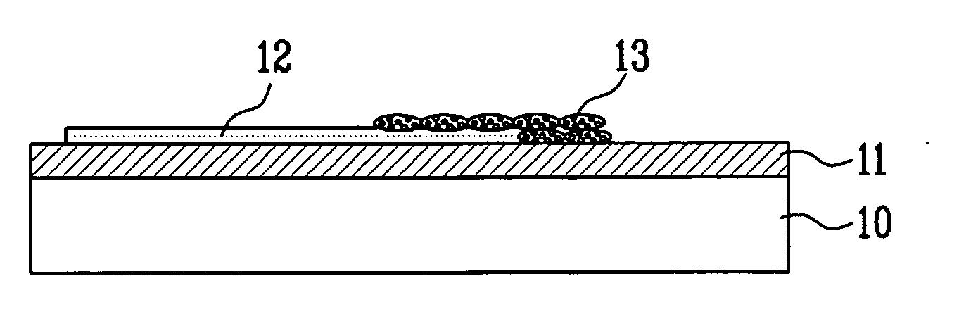
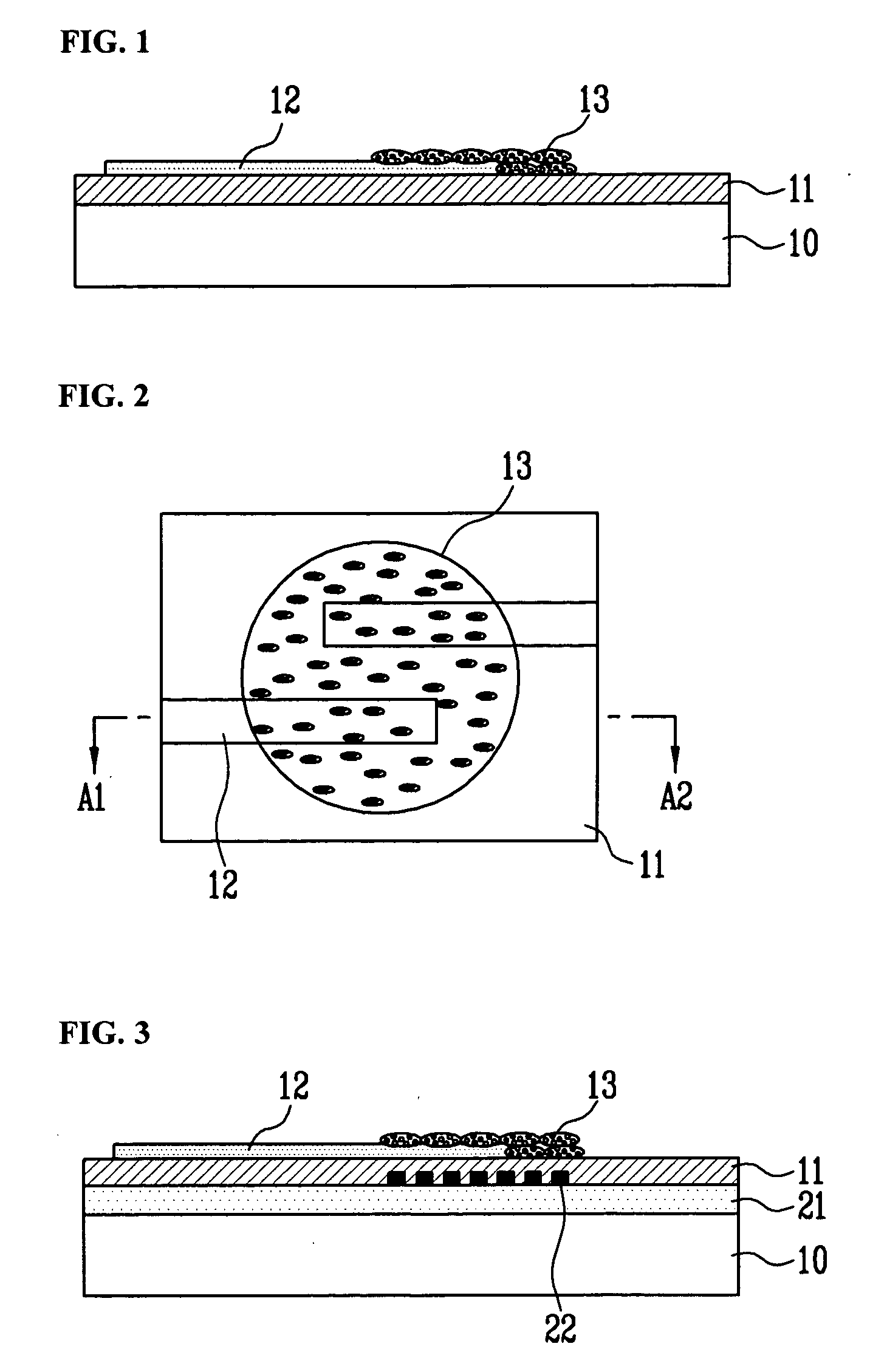
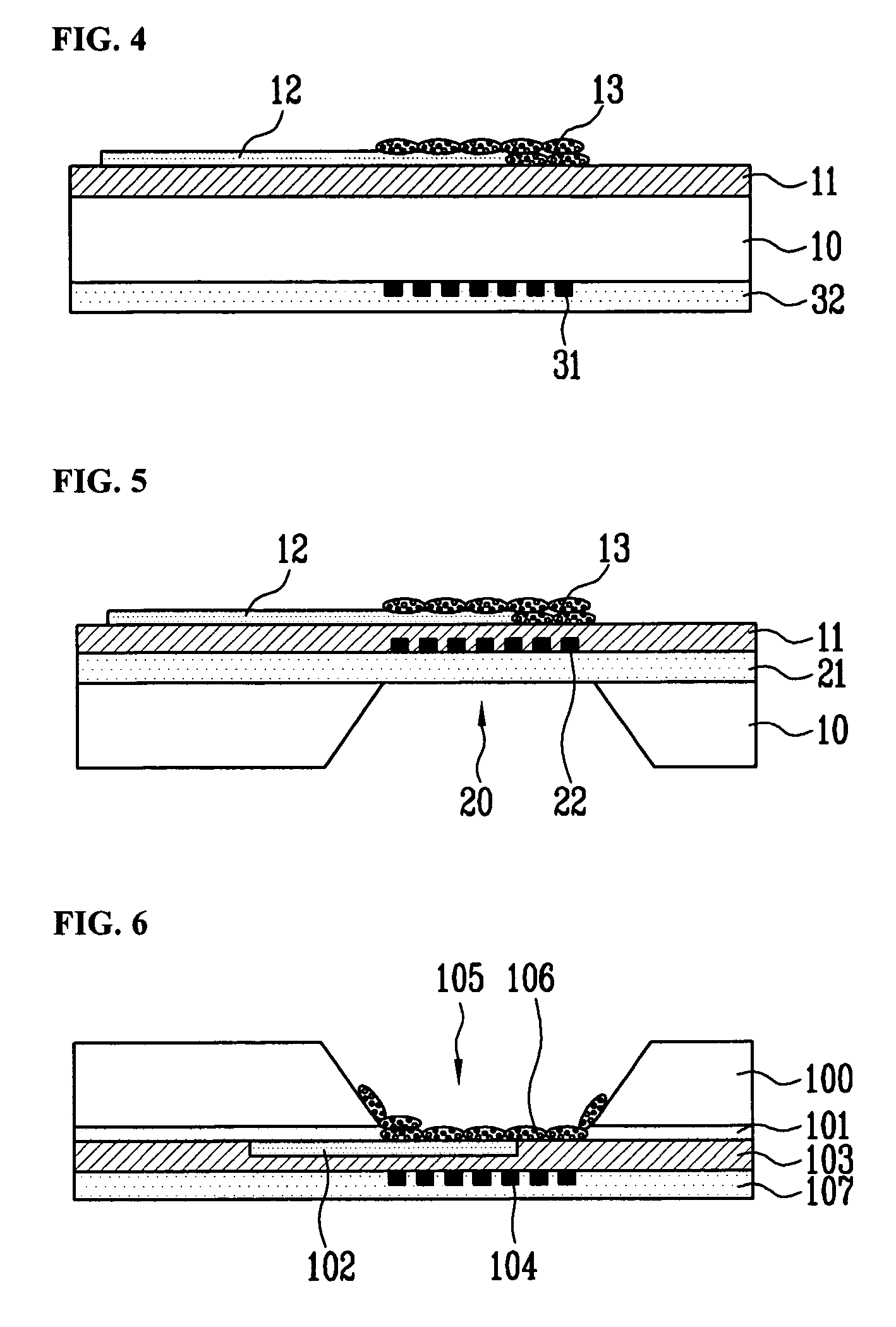
[0042]FIG. 1 is a cross-sectional view of a chemical sensor in accordance with the present invention.
[0043] An insulating layer 11 is formed on a substrate 10, and a sensing electrode 12 is formed on the insulating layer 11. In addition, a sensing layer 13 is formed on the insulating layer 11 including the sensing electrode 12.
[0044] The substrate 10 may employ a silicon substrate, a GaAs substrate, a glass substrate, a ceramic substrate, a plastic substrate, and so on.
[0045] The insulating layer 11 functions to maintain electrical insulation between the sensing electrode 12 and a lower structure, and physically support the sensing electrode 12 and the sensing layer 13. Therefore, preferably, the insulating layer 11 is formed of an oxide layer, a nitride layer or a stacked layer of an oxide layer and a nitride layer which has high insulation performance, high structural stability, and excellent adhesive performance between upper and lower layers, without generating problems such a...
second embodiment
[0052]FIG. 3 is a cross-sectional view of a chemical sensor in accordance with the present invention. In the structure of the chemical sensor of FIG. 1, a heater 22 made of metal lines is formed in the insulating layer 11 under the sensing layer 13, and isolated from the substrate 10 by interposing an isolation layer 21.
[0053] The heater 22 may be formed of a thin layer or a thick layer of a conductive material. In the case of the thin layer, the heater12 is deposited using a vacuum deposition method and then patterned in a microscopic heater shape, and in the case of the thick layer, a mixture of conductive metal particles and organic materials is screen-printed. The conductive material typically employs Au, Pt, Al, Mo, Ag, TiN, W, Ru, Ir, poly-Si and so on. An auxiliary material may be formed to improve adhesion between a deposition subject and the metal material before deposition of the conductive material. For example, Cr or Ti may be formed on glass or silicon to improve adhesi...
third embodiment
[0055]FIG. 4 is a cross-sectional view of a chemical sensor in accordance with the present invention. In the structure of the chemical sensor of FIG. 1, a heater 31 made of metal lines is formed at a bottom surface of the substrate 10 under the sensing layer 13, and a passivation layer 32 is formed on the bottom surface 10 of the substrate 10 including the heater 31. In the embodiment, preferably, the substrate 10 uses a ceramic substrate such as alumina having excellent thermal conductivity and insulation characteristics.
[0056] The passivation layer 32 functions to prevent the heat generated from the heater 31 and the electricity flowing through the heater 31 from leaking to the exterior. Therefore, the passivation layer 32 may be formed of an oxide layer or a nitride layer having an insulation characteristic and a fine structure, or may be formed of a thick layer using insulating paste.
PUM
 Abstract
Description
Claims
Application Information


