Communications test receiver

Inactive Publication Date: 2006-11-09
AVAGO TECH WIRELESS IP SINGAPORE PTE
View PDF7 Cites 0 Cited by
  • Summary
  • Abstract
  • Description
  • Claims
  • Application Information

AI Technical Summary

Benefits of technology

[0025] Because of the relative simplicity of the arrangement, the register and associated circuitry for clocking out or otherwise presenting the data values at the output may be provided on the same integrated circuit as used for other functions within the test receiver unit. Preferably, the delay line(s) used for the register is/are the same delay line(s) used by the equaliser.
[0026] In one embodiment of the invention, the test receiver unit is a functional receiver unit for receiving data as part of an optical communications system.
[0027] Because the register is relatively simple and will consume little power compared with the total electrical power consumed by the test receiver unit, the unit may be arranged so that the register is always storing and presenting at an output data values. However, it may be desirable to disable the testing function of the test receiver unit when the unit is being used to receive data, or vice versa.
[0028] The test receiver unit may comprise means by which the test receiver unit is temporarily placed in a testing mode of operation during which the

Problems solved by technology

A transmitted signal may be subject to numerous sources of noise and distortion, both in the generation of the signal and its transmission through a communications channel.
For example, sources of noise in an optical transmitter or receiver include thermal noise and shot noise.
A receiver section of the receiver may also use an avalanche photodiode for high sensitivity, but this will introduce avalanche photodiode noise.
The generation of an optical signal will in general be subject to other sources of noise or drift.
Such feedback will cause rapid changes in system distortion, which can close the eye pattern in a received signal.
In this case the system suffers from intersymbol interference (ISI), which in conjunction with system noise, increases the bit error rate (BER) of the received signal.
ISI is interference resulting from the data pattern itself.
Similarly, electrical signals

Method used


Image

  • Communications test receiver
  • Communications test receiver
  • Communications test receiver

Examples


Example

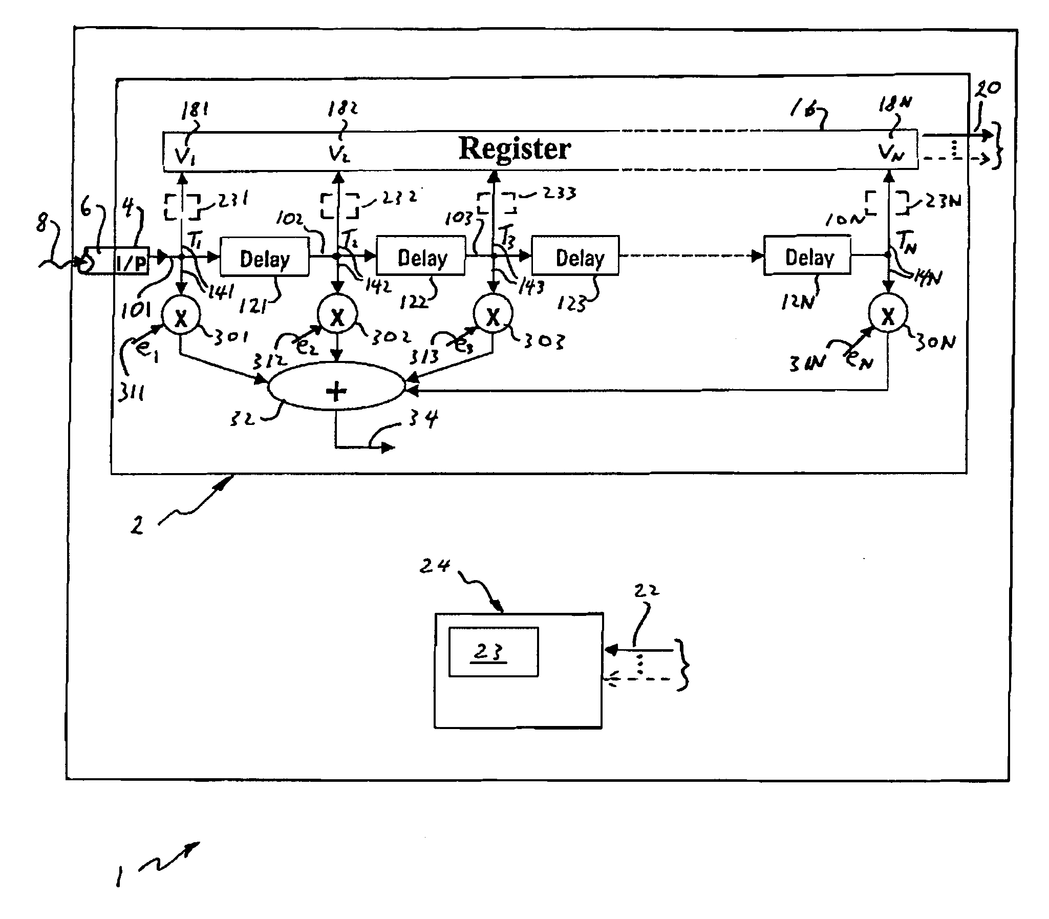
[0047]FIG. 1 shows a test system 1 having a test receiver unit 2 for receiving and testing an input optical signal received from an optical fibre 6. The test receiver unit has a photoreceiver input (I / P) 4 for receiving optical radiation 8 from the fibre 6. The optical radiation 8 is modulated to carry an optical signal. The input 4 is conventional, and so will not be described or illustrated in detail, but includes a photodetector and associated amplification circuitry for converting the optical radiation into an electrical signal 101. The electrical signal 101 in this example includes non-random distortion, for example inter-symbol interference.

[0048] The test receiver unit 2 includes at least one delay line 121 to 12N arranged to delay the electrical signal 101, at least two taps (T1 to TN) 141 to 14N from the delay lines 121-12N by which access is had to delayed electrical signals 102-10N and optionally also to the un-delayed signal 101. A register 16 is connected to the delay ...


PUM


Abstract

Distortion of an optical signal transmitted over a fibre optic link is characterized by a receiver including a photodetector for converting optical radiation into an electrical signal. A delay line delays the electrical signal. At least two delay line taps drive a register that stores plural values corresponding with different delayed replicas of the electrical signal. Signals commensurate with the values are externally provided to a signal distortion analyser for analysis of the values to determine the optical signal distortion.

Description

RELATED APPLICATIONS [0001] The present application is based on, and claims priority from, British Application Serial Number 0502185.2, filed Feb. 3, 2005, the disclosure of which is hereby incorporated by reference herein in its entirety BACKGROUND [0002] a. Field of the Invention [0003] The present invention relates to a test receiver unit for receiving and testing a signal transmitted over a communications link, and to a communications system and method that uses a test receiver unit to characterise distortion in a the signal. The signal may be an electrical signal transmitted over an electrical communications link, or an optical signal transmitted over an optical communications link. [0004] b. Related Art [0005] A transmitted signal may be subject to numerous sources of noise and distortion, both in the generation of the signal and its transmission through a communications channel. For example, sources of noise in an optical transmitter or receiver include thermal noise and shot...

Claims


Application Information

Patent Timeline
IPC IPC(8): G01R23/20H04L1/24H04L25/03
CPCH04L1/24H04L25/03025H04L2025/03808H04L2025/03471H04L25/03038
Inventor HEALY, DAVIDCRONIN, RICHARDBOTHWELL, ANDREW
Owner AVAGO TECH WIRELESS IP SINGAPORE PTE
Why Eureka
Try Eureka