Pad structure, pad layout structure, and pad layout method in semiconductor devices

Active Publication Date: 2006-11-16
SAMSUNG ELECTRONICS CO LTD
View PDF11 Cites 14 Cited by
  • Summary
  • Abstract
  • Description
  • Claims
  • Application Information

AI Technical Summary

Benefits of technology

[0033] Accordingly, one exemplary embodiment of the invention provides a pad layout structure in a semiconductor device, which is capable of obtaining a high integration by increasing a pad pitch in a limited region so as to form additional peripheral circuits in a region of the device formerly occupied by unused bonding pads. In the pad layout structure, the relativ

Problems solved by technology

The pad structure can reduce problems that otherwise can occur with the excessive generation of particles through conta

Method used


Image

  • Pad structure, pad layout structure, and pad layout method in semiconductor devices
  • Pad structure, pad layout structure, and pad layout method in semiconductor devices
  • Pad structure, pad layout structure, and pad layout method in semiconductor devices

Examples


Example

[0069] The present invention will now be described more fully hereinafter with reference to the accompanying drawings, in which preferred embodiments of the invention are shown. This invention may, however, be embodied in different forms and should not be construed as limited to the embodiments set forth herein. Like numbers refer to like elements throughout the specification.

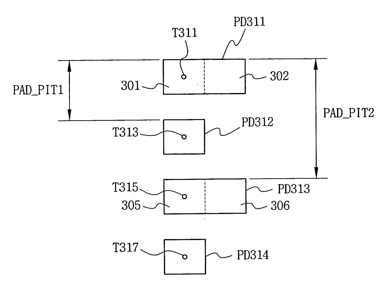
[0070]FIG. 5 is a schematic view illustrating a pad layout structure in a semiconductor device according to one exemplary embodiment of the invention.

[0071] Referring to FIG. 5, pads PD311, PD312, PD313 and PD314, and a pad pitch PAD_PIT1, PAD_PIT2, are shown.

[0072] In semiconductor devices, particularly in a semiconductor memory device as an example, pads formed in a pad region of the semiconductor memory device enable the semiconductor memory device to be electrically connected with external devices. Signals concerning command input and data read and write operations are input to the device, or are output ...


PUM


Abstract

In a layout structure of pads and a structure of pad used for a test or wire bonding of a semiconductor device, a size of at least one or more non-wire bonding pads is relatively small as compared with a size of at least one or more pads to be used for wire bonding of the semiconductor device. In the pad structure, a pad includes a wire bonding region that has an embossed surface for a portion of top metal layer within a determined pad size to improve the bonding process, and a probe tip contact region that does not have the embossed surface for a surface portion of the top metal layer within the determined pad size, so as to reduce wear of probe tip during testing of the device. Pad pitch can thereby be increased within a limited region, and peripheral circuits can be further formed in regions that would have been occupied in a conventional pad formation region. Higher integration of semiconductor devices and reduced wear of probe tip in probing is thereby realized.

Description

RELATED APPLICATIONS [0001] This application claims priority to Korean Patent Application No. 10-2005-0013949, filed on Feb. 21, 2005 and to Korean Patent Application No. 10-2005-0016422, filed on Feb. 28, 2005, in the Korean Intellectual Property Office, the disclosures of which are incorporated herein by reference, in their entirety. BACKGROUND OF THE INVENTION [0002] 1. Technical Field of the Invention [0003] The present invention relates to a semiconductor device, and more particularly, to a pad structure, pad layout structure and layout method in a semiconductor device. [0004] 2. Description of the Related Art [0005] In semiconductor devices, particularly semiconductor memory devices, pads are provided to electrically connect a semiconductor memory device to external devices. Through the pads, signals including command signals, data read signals, and data write signals are input to or output by the device. [0006] There is a continuing trend toward high integration in semiconduc...

Claims


Application Information

Patent Timeline
IPC IPC(8): H01L23/48
CPCH01L22/32H01L2224/0603H01L24/05H01L24/06H01L2224/04042H01L2224/05093H01L2224/05094H01L2224/05095H01L2224/45144H01L2924/01004H01L2924/01005H01L2924/01046H01L2924/01079H01L2924/01082H01L2924/19041H01L2924/01006H01L2924/01033H01L2924/01068H01L2224/05553H01L2924/00014H01L24/03H01L2224/05552H01L2924/13091H01L2224/48H01L2924/00
Inventor KIM, NA-RAESON, TAE-SIKOH, HEE-JOONGKWAK, BYUNG-HEONJOO, JAE-HOONKIM, HYUNG-DONGJANG, YOUNG-MIN
Owner SAMSUNG ELECTRONICS CO LTD
Why Eureka
Try Eureka