Offset adjusting circuit and operational amplifier circuit

Inactive Publication Date: 2006-11-16
SHARP KK
View PDF6 Cites 18 Cited by
  • Summary
  • Abstract
  • Description
  • Claims
  • Application Information

AI Technical Summary

Benefits of technology

[0028] An object of the present invention is to provide an offset adjusting circuit which is capable of adjusting

Problems solved by technology

However, in an actual LSI, due to a production-caused variation, there is a random variation in the voltages respectively output from the operation amplifiers in the LSI.
Thus, the line-by-line variation in the drive voltages applied to the data lines causes a non-uniform displaying.
These methods, however, lead to an increase in the size of a chip and in the production cost, when an offset adjusting circuit is formed into an LSI.
However, in either

Method used


Image

  • Offset adjusting circuit and operational amplifier circuit
  • Offset adjusting circuit and operational amplifier circuit
  • Offset adjusting circuit and operational amplifier circuit

Examples


Embodiment Construction

[0048] The following describes an embodiment of the present invention with reference to the drawings.

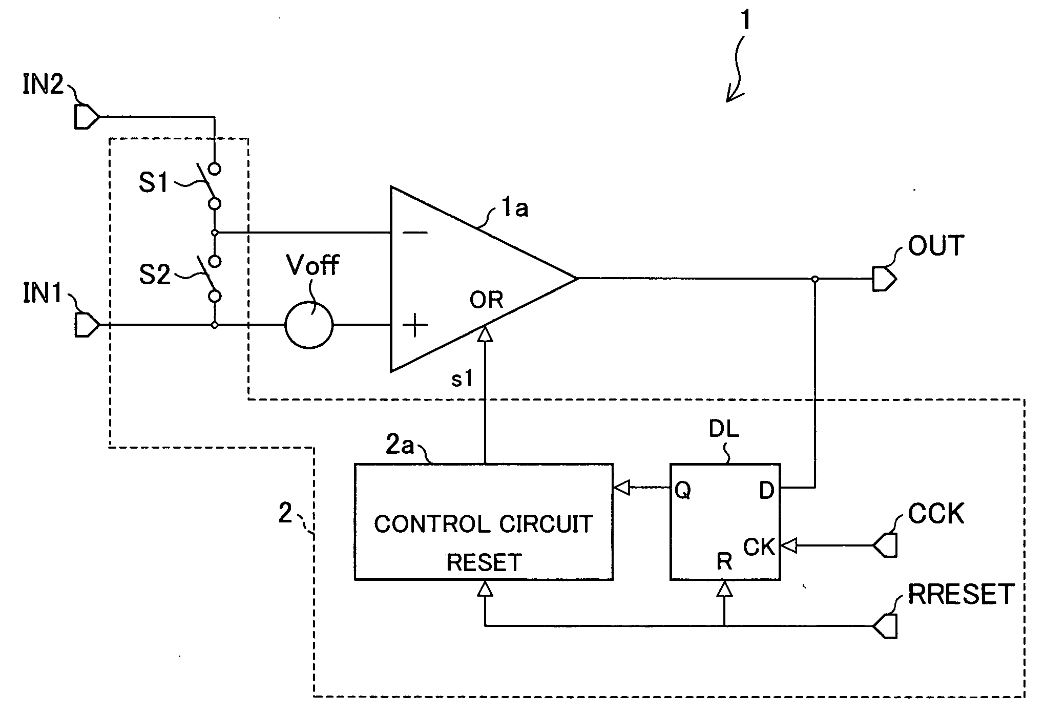
[0049]FIG. 1 is a circuit block diagram of an embodiment in accordance with the present invention, and is illustrating a configuration of an operational amplifier circuit including a first offset adjusting circuit.

[0050] An operational amplifier circuit 1 includes: an operational amplifier 1a; an offset adjusting circuit 2; a common phase input terminal IN1; a negative-phase input terminal IN2; and an output terminal OUT. Note that, an offset of an output voltage of the operational amplifier la is represented by a voltage source Voff which serves as a power source: i.e., an input offset of an inphase input signal. This voltage source Voff is provided between a non-inverting input terminal of the operational amplifier 1a and the common phase input terminal IN1. Accordingly, a cause of an offset is removed from the operational amplifier 1a itself illustrated in the figure. However, a...


PUM


Abstract

The present invention provides an offset adjusting circuit and an operational amplifier circuit. In the operational amplifier circuit (1), a switching element (S1) is closed and a switching element (S2) is opened. The latch circuit DL latches an output voltage of an operational amplifier (1a), and output a Q-output in accordance with the output voltage. The control circuit (2a) inputs an offset adjustment signal s1 to an offset adjustment input terminal OR of the operational amplifier (1a). Then, the latch circuit DL latches the output voltage having been subjected to the offset adjustment, and the offset adjustment signal s1 is finely adjusted for adjusting the remaining offset. In this way, the offset in the output voltage of the operational amplifier (1a) is quantized in accordance with the number of times the latching operation has been performed, and is stored in the control circuit (2a) in the form of a binary logical signal.

Description

[0001] This Nonprovisional application claims priority under 35 U.S.C. § 119(a) on Patent Application No. 2005 / 133212 filed in Japan on Apr. 28, 2005, the entire contents of which are hereby incorporated by reference. FIELD OF THE INVENTION[0002] The present invention relates to an offset adjustment for an operational amplifier circuit. Particularly, the present invention is for reducing a variation in a random offset of an output operational amplifier circuit in a TFT-LCD source driver circuit, which offset is caused by a production-caused variation. BACKGROUND OF THE INVENTION [0003] In general, a TFT-LCD drive circuit drives a liquid crystal panel by (i) digitally processing a display signal, and (ii) converting, with a use of a DA converter, the digitally processed display signal into an analogue voltage according to a display tone of the display signal In recent years, a load of the liquid crystal panel has been increasingly becoming large for a given drive circuit, with an inc...

Claims


Application Information

Patent Timeline
IPC IPC(8): H03F1/02
CPCH03F3/45192H03F3/45475H03F3/45928H03F2203/45058H03F2203/45726H03F2203/45588H03F2203/45616H03F2203/45634H03F2203/45681H03F2203/45101H03F3/34
Inventor NAKAO, TOMOAKI
Owner SHARP KK
Why Eureka
Try Eureka