Method of fabricating silicon-doped metal oxide layer using atomic layer deposition technique

Inactive Publication Date: 2006-11-16
SAMSUNG ELECTRONICS CO LTD
View PDF5 Cites 379 Cited by
  • Summary
  • Abstract
  • Description
  • Claims
  • Application Information

AI Technical Summary

Benefits of technology

[0015] Therefore, the present invention provides a method of fabricating a silicon-doped metal oxide layer on a suitable semiconductor substrate, wherein the method is capable of precisely

Problems solved by technology

Efforts to reduce such dielectrics in both overall size and thickness have led, however, to many difficulties in fabrication.
For example, if a thickness of a gate dielectric layer as one component element of the transistor is formed too thin, there may result a deterioration in the insulation characteristics of the gate dielectric layer.
In the case where a thickness of the silicon oxide layer is reduced to about 15 or less, it has been reported that there occurs a rapid increase in leakage current apparently caused by a direct tunneling effect in a gate electrode.
As widely known, the PVD technique has serious limitations because of a poor step coverage and poor interface characteristics with a silicon substrate.
The CVD technique also has serious limitations because of the need to use high temperatures to form thin films, and because of limitations in being able to precisely control the thickness of the thin film within a tolerance of several.
Further, because a composition rat

Method used


Image

  • Method of fabricating silicon-doped metal oxide layer using atomic layer deposition technique
  • Method of fabricating silicon-doped metal oxide layer using atomic layer deposition technique
  • Method of fabricating silicon-doped metal oxide layer using atomic layer deposition technique

Examples


Embodiment Construction

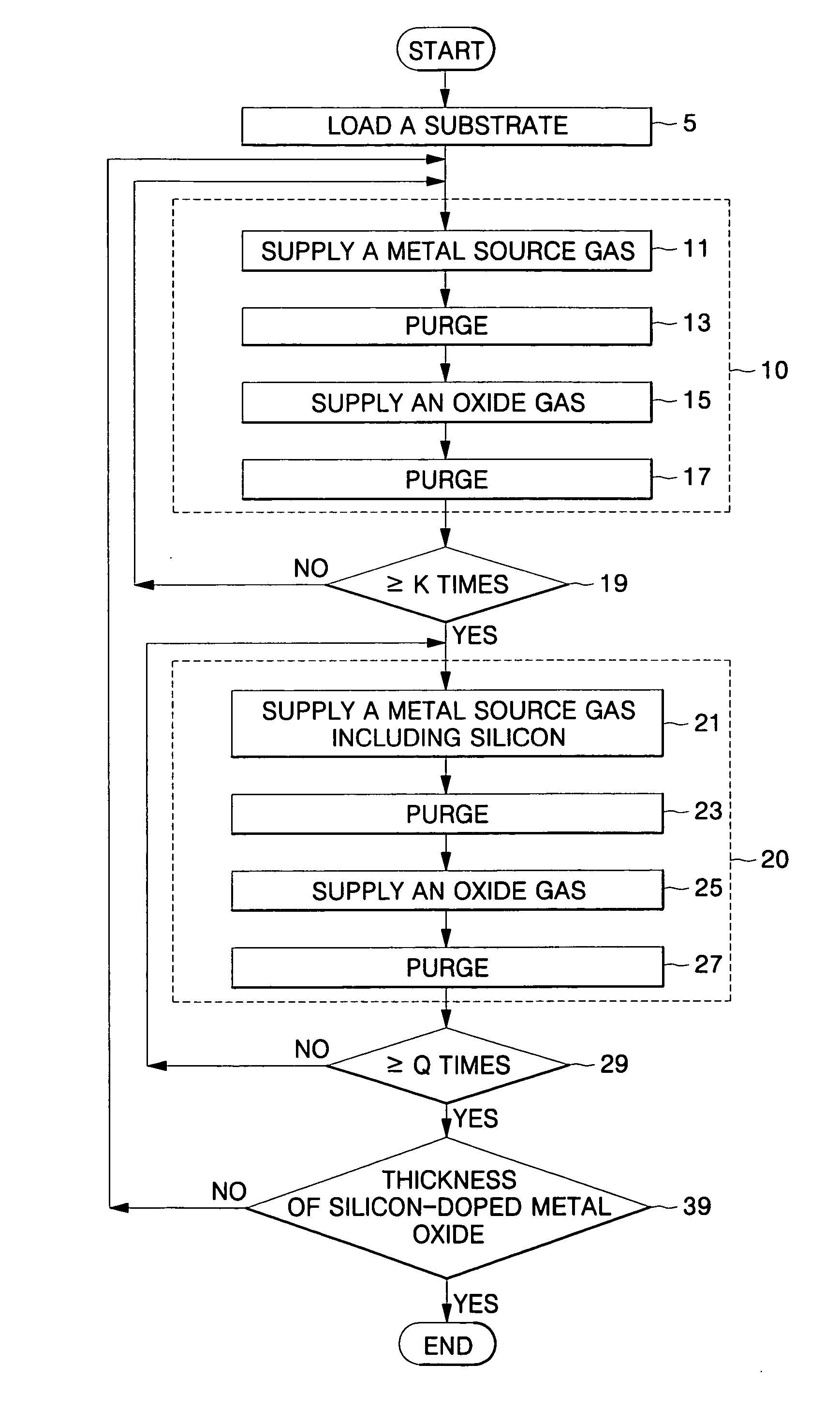
[0030] The present invention will now be described more fully hereinafter with reference to the accompanying drawings, in which preferred embodiments of the invention are shown. It will be understood, however, that this invention may be embodied in many different forms and should not be construed as being limited to the embodiments set forth herein. Rather, these embodiments are provided so that this disclosure will be thorough and complete, and will fully convey the scope of the invention to those skilled in the art. Like numbers in the drawings are used to refer to like elements throughout the specification.

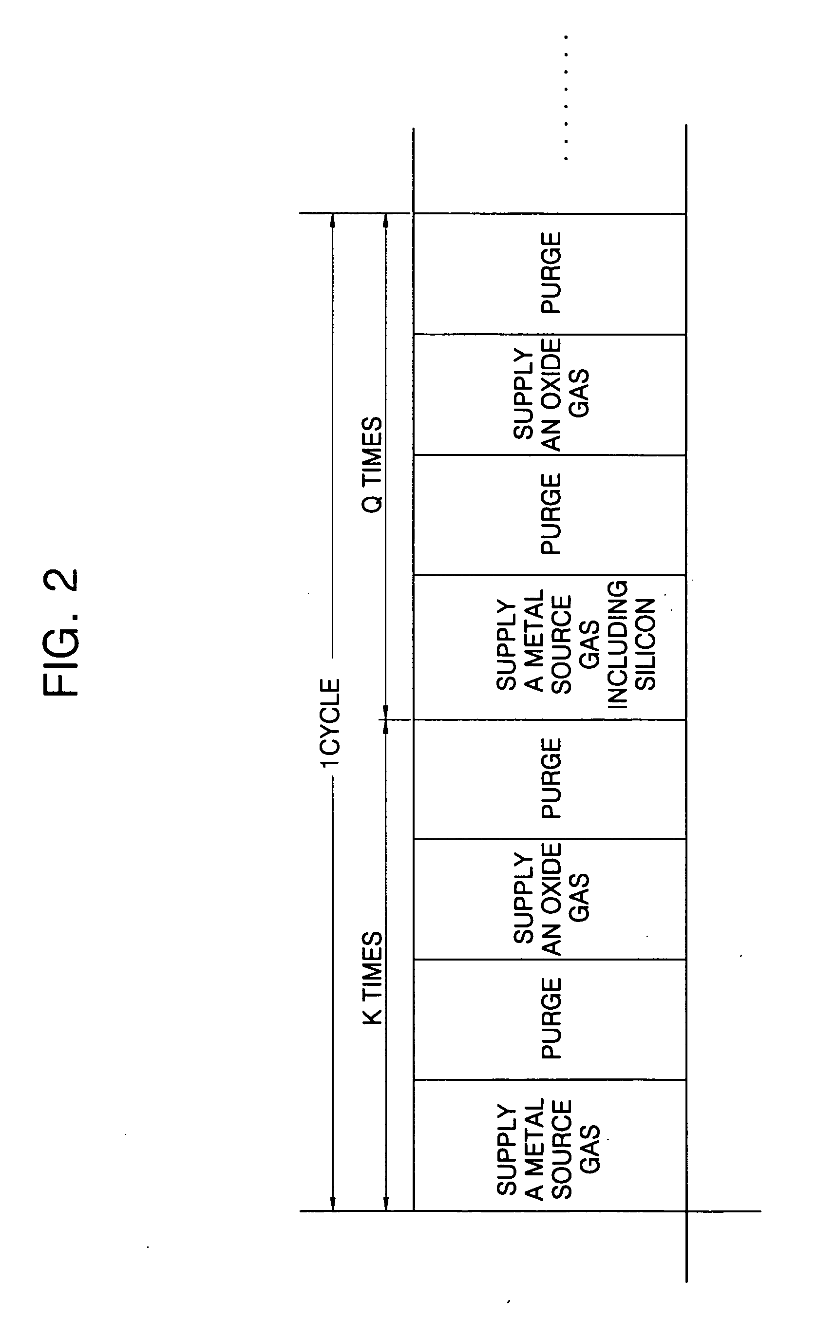
[0031]FIG. 1 is a process flow chart generally illustrating a method of fabricating a silicon-doped metal oxide layer using an ALD technique according to the present invention, and FIG. 2 is a diagram of a single complete layer deposition cycle illustrating a method of fabricating a silicon-doped metal oxide layer using an ALD technique according to the present invention.

[003...


PUM

PropertyMeasurementUnit
Temperatureaaaaaaaaaa
Thicknessaaaaaaaaaa

Abstract

There are provided methods of fabricating a silicon-doped metal oxide layer on a semiconductor substrate using an atomic layer deposition technique. The methods include an operation of repeatedly performing a metal oxide layer formation cycle K times and an operation of repeatedly performing a silicon-doped metal oxide layer formation cycle Q times. At least one of the values K and Q is an integer of 2 or more. K and Q are integers ranging from 1 to about 10 respectively. The metal oxide layer formation cycle includes the steps of supplying a metal source gas to a reactor containing the substrate, and then injecting an oxide gas into the reactor. The silicon-doped metal oxide layer formation cycle includes supplying a metal source gas including silicon into a reactor containing the substrate, and then injecting an oxide gas into the reactor. The sequence of operations of repeatedly performing the metal oxide layer formation cycle K times, followed by repeatedly performing the silicon-doped metal oxide layer formation cycle Q times, is performed one or more times until a silicon-doped metal oxide layer with a desired thickness is formed on the substrate. In addition, a method of fabricating a silicon-doped hafnium oxide (Si-doped HfO2) layer according to a similar invention method is also provided.

Description

CROSS-REFERENCE TO RELATED APPLICATION [0001] The present application is a continuation-in-part of U.S. patent application Ser. No. 11 / 127,748, filed May 12, 2005, which is based on U.S. Provisional Application No. 60 / 618,106, filed Oct. 13, 2004, the contents of which are incorporated in their entireties herein by reference. The present application claims the priority of Korean Patent Application No 2005-0002984, filed Jan. 12, 2005, the content of which is hereby incorporated herein by reference in its entirety.BACKGROUND OF INVENTION [0002] 1. Technical Field [0003] The present invention relates to a method of fabricating a thin layer of a semiconductor device, and more particularly, to a method of fabricating a silicon-doped metal oxide layer on a semiconductor substrate using an atomic layer deposition (ALD) technique. [0004] 2. Discussion of the Related Art [0005] With growing demand for highly-integrated semiconductor devices, a transistor and a capacitor as component semicon...

Claims


Application Information

Patent Timeline
IPC IPC(8): C23C16/00
CPCC23C16/401C23C16/45531C23C16/45529
Inventor DOH, SEOK-JOORHEE, SHI-WOOKIM, JONG-PYOLEE, JUNG-HYOUNGLEE, JONG-HOKIM, YUN-SEOK
Owner SAMSUNG ELECTRONICS CO LTD
Why Eureka
Try Eureka