Thermal lamination module

a technology of thermal lamination and module, which is applied in the field of thermal management devices, can solve the problems of increasing the “cost” of heat dissipation, increasing the risk of failure or malfunction of electronic components at higher temperatures, and reducing the efficiency of thermal management, so as to improve thermal management and reduce friction. the effect of heat dissipation

Inactive Publication Date: 2006-11-23
PARKER HANNIFIN CORP
View PDF5 Cites 24 Cited by
  • Summary
  • Abstract
  • Description
  • Claims
  • Application Information

AI Technical Summary

Benefits of technology

[0017] There is a need for an improved thermal laminate for dissipating heat in the vicinity of a PCMCIA card. The thermal laminate of this invention utilizes sliding contacts for proper movement within the assembly, and a close mating between a heat sink surface and the PCMCIA card for better thermal management. Moreover, the thermal laminate provides soft conformal, low friction interfacing surfaces which are highly desirable for the thermal laminate when in use.

Problems solved by technology

Designers and manufacturers are now facing the challenge of dissipating the heat which is ohmic in nature or otherwise generated in built in electronic components.
Each of these increases in processing speed and power generally carry with it a “cost” of increased heat dissipation.
The electronic components are more prone to failures or malfunctioning at higher temperatures.
The electronic components are small sized and the generation of even a moderate amount of heat can create excessive operating temperatures in such components, which can be very detrimental.
However, a simple circulation of air is typically insufficient to adequately cool the high powered and densely packed electronic components, such as PCMCIA cards, or other expansion cards.
In portable electronic devices, however, the cooling of a PCMCIA card is not a simple matter.

Method used


Image

  • Thermal lamination module
  • Thermal lamination module
  • Thermal lamination module

Examples


second embodiment

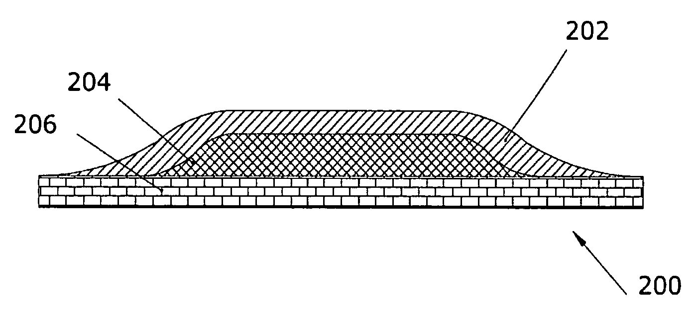
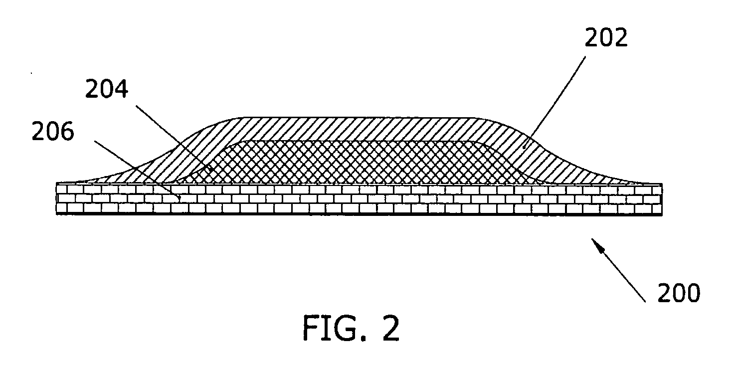
[0048] In a second embodiment as depicted in FIG. 5, a thermal laminate 500 includes a top tedlar film layer 502, a middle gap filler layer 504, and a bottom copper foil layer 506. The top film layer 502 provides an interface to the thermal laminate 500. The middle gap filler layer 504 is disposed underneath the top film layer 502. The middle gap filler layer 504 provides a thermal pathway for the heat radiation. The bottom copper foil layer 506 is disposed underneath the middle gap filler layer 504. The bottom copper foil layer 506 provides a grip to the top film layer 502 and a middle gap filler layer 504. The copper foil is ideal for printed wiring board modification and repair. The copper foil is also designed for use as electro-magnetic interference (EMI) and radio-frequency interference (RFI) shielding on the electronic devices or other small electromagnetic components, such as transformer and reactor coils, instruments and control motors. The copper foil has outstanding adhes...

third embodiment

[0049] In a third embodiment, a thermal laminate 600 includes a top tedlar film layer 602 and a gap filler layer 604 as shown in FIG. 6. The top film layer 602 provides enveloping edges beyond the gap filler layer 604. The top film layer 602 provides an interface to the thermal laminate 600. The gap filler layer 604 is disposed underneath the top film layer 602. The gap filler layer 604 provides a thermal pathway to heat radiation emitted from the PCMCIA card. The gap filler layer 604 also provides a grip to the top film layer 602.

fourth embodiment

[0050] In a fourth embodiment, a thermal laminate 700 includes a top tedlar film layer 702, a middle gap filler layer 704 and a thermal adhesive bottom layer 706. The middle gap filler layer 704 and the thermal adhesive bottom layer 706 can be configured for different sizes as shown in FIG. 7. The top tedlar film layer 702 is wrapped around to provide enveloping edges over middle gap filler layer 704 and the bottom layer 706. The top film layer 702 provides an interface for the thermal laminate 700. The middle gap filler layer 704 is disposed underneath the top film layer 702. The middle gap filler layer 704 provides a thermal pathway for heat radiation. The bottom layer 706 is disposed underneath the middle gap filler layer 704 to provide a grip for the top film layer 702 and a middle gap filler layer 704.

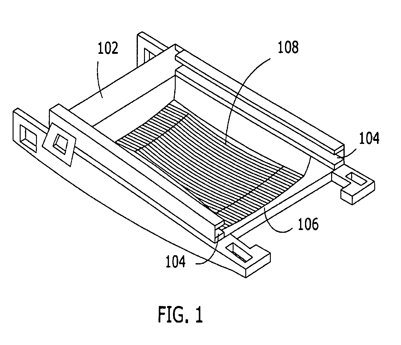
[0051]FIG. 4 represents the assembly 102 installed on an electronic device having the present thermal laminate, the heat sink 108 and a PCMCIA card 402 positioned thereon, in acco...


PUM

PropertyMeasurementUnit
thicknessaaaaaaaaaa
thicknessaaaaaaaaaa
operating temperaturesaaaaaaaaaa

Abstract

The present invention discloses a thermal laminate for the dissipation of heat generated in the vicinity of an installed PCMCIA card. The thermal laminate includes a top film layer, a middle gap filler layer and a bottom layer. The top film layer provides a protective, non-resistive, low friction surface with a soft conformal interface for enhancing the workability of the thermal laminate. The middle gap filler layer is disposed underneath the top film layer and provides a conformal thermal pathway for the heat radiation emitted from the installed PCMCIA card. The bottom layer is disposed underneath the middle gap filler layer and provides a grip to the middle gap filler layer and the top film layer. The bottom layer is made from either a thermal adhesive layer or a copper foil layer. The thermal laminate utilizes sliding contacts for proper housing between a PCMCIA card surface and a heat sink surface to provide better thermal management within an assembly.

Description

CROSS-REFERENCE TO RELATED APPLICATIONS [0001] This application claims the benefit of priority from U.S. Provisional Application No. 60 / 682,500, filed on May 19, 2005, which is incorporated herein by reference in its entirety.BACKGROUND OF THE INVENTION [0002] The present invention relates to thermal management devices for electronic circuit boards, and more specifically; to a thermal laminate providing dissipation of heat generated on and around a PCMCIA card installed in an electronic device, such as a laptop, a notebook, a sub-notebook, cellular phone, etc. [0003] In recent years electronic devices have become smaller and more densely packed. Designers and manufacturers are now facing the challenge of dissipating the heat which is ohmic in nature or otherwise generated in built in electronic components. Thermal management refers to the ability to keep temperature-sensitive elements in an electronic device within a prescribed operating temperature. Thermal management has evolved t...

Claims


Application Information

Patent Timeline
Patent Type & Authority Applications(United States)
IPC IPC(8): B32B3/02
CPCB32B3/02Y10T428/239B32B7/02B32B15/06B32B15/20B32B25/02B32B25/08B32B25/20B32B27/304B32B2250/03B32B2250/44B32B2262/101B32B2264/107B32B2307/302B32B2307/308B32B2307/54B32B2307/558B32B2307/5825B32B2307/714B32B2307/732B32B2307/746B32B2457/00B32B2457/08H05K7/20472H01L2924/0002B32B3/04Y10T428/23H01L2924/00H05K7/20481F28F7/00
Inventor BUNYAN, MICHAEL H.
Owner PARKER HANNIFIN CORP
Why Eureka
Try Eureka