

Light-emitting element and light-emitting device
- Summary
- Abstract
- Description
- Claims
- Application Information
AI Technical Summary
Benefits of technology
Problems solved by technology
Method used
Image

Examples
embodiment modes
[0060] Hereinafter, the embodiment modes of the present invention will be described with reference to the accompanying drawings. The present invention is not limited to the following description, and it is easily understood by those skilled in the art that modes and details herein disclosed can be modified in various ways without departing from the spirit and the scope of the present invention. It should be noted that the present invention should not be interpreted as being limited to the description of the embodiment modes to be given below. Note that in structures of the present invention to given below, the same reference numerals are used for the same portions or the portions having the same functions in some cases.
embodiment mode 1
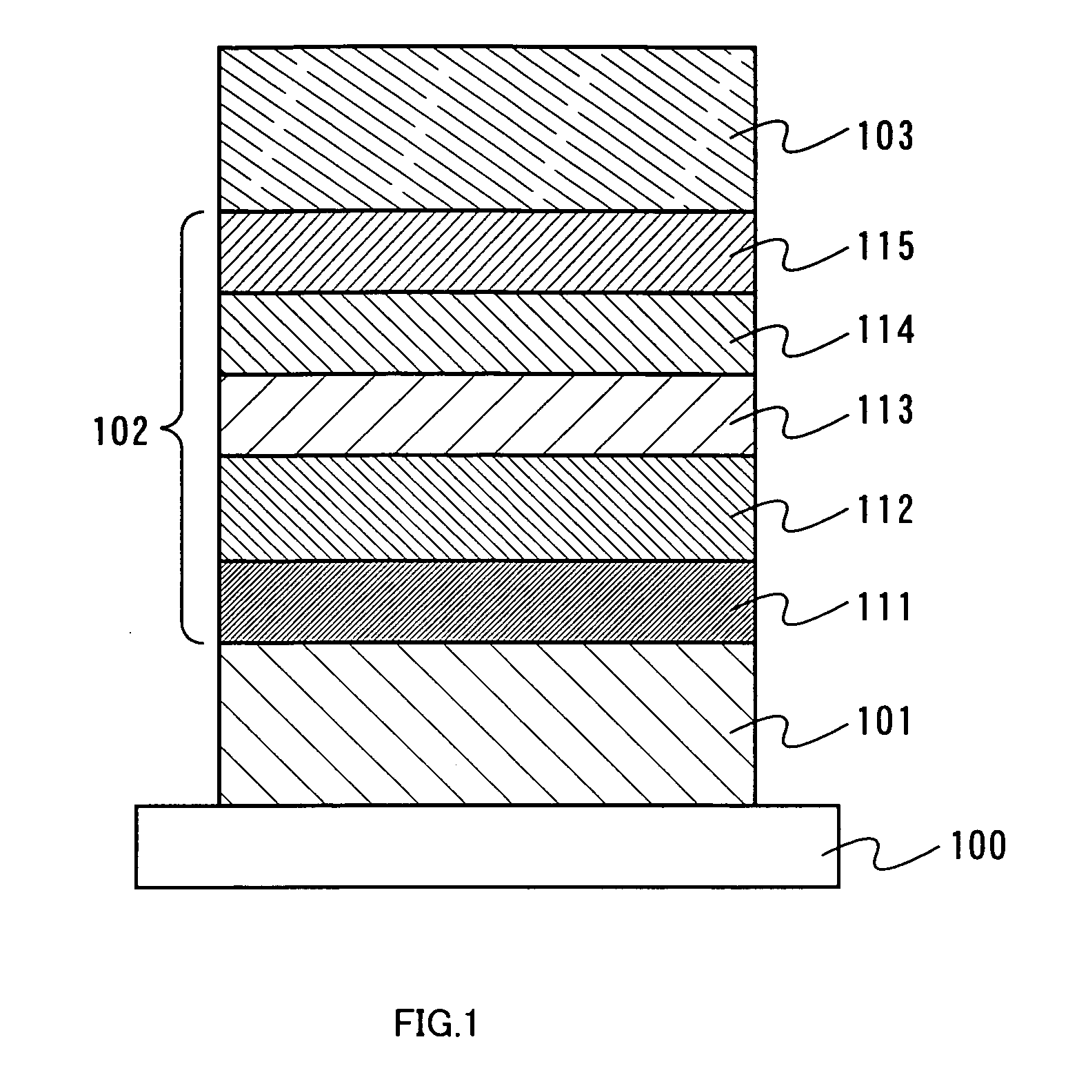
[0061] Embodiment Mode 1 will describe one mode of a light-emitting element of the present invention with reference to FIG. 1. As shown in FIG. 1, a first electrode 101 is formed over a substrate 100, a layer including a light-emitting substance 102 is formed over the first electrode 101, and a second electrode 103 is formed thereover. In addition, the layer including a light-emitting substance 102 is formed by stacking a plurality of layers, and the structure of Embodiment Mode 1 includes a hole injecting layer 111, a hole transporting layer 112, a light-emitting layer 113, an electron transporting layer 114 and an electron injecting layer 115. These layers can be formed by an evaporation method or a coating method.
[0062] As a material used for the substrate 100, quartz, glass, plastic, a flexible substrate or the like can be used, for example. It is to be noted that other materials may be used, so long as they can function as a support in a manufacturing process of a light-emitti...
embodiment mode 2
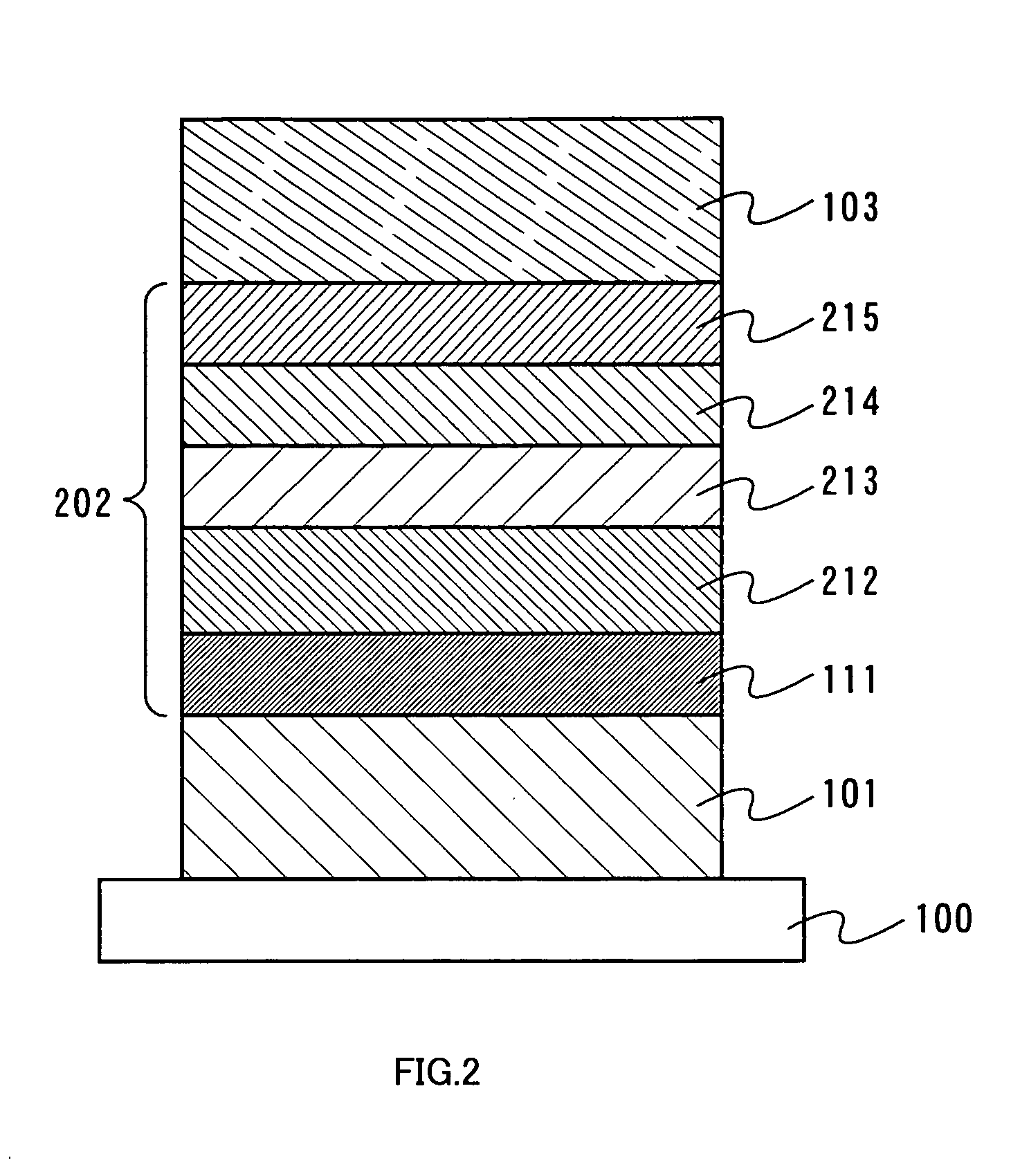
[0082] One mode of a light-emitting element of the present invention will be described with reference to FIG. 2. As shown in FIG. 2, a first electrode 101 is formed over a substrate 100, a layer including a light-emitting substance 202 is formed over the first electrode 101, and a second electrode 103 is formed thereover. Note that a different point from Embodiment Mode 1 is that a material having a higher triplet excitation energy than an organometallic complex serving as a light-emitting substance is used, for a hole transporting layer, a host included in a light-emitting layer, and an electron transporting layer. As for the similar elements to those of Embodiment Mode 1 are shown by the common reference numerals and detailed description is omitted. In addition, in this embodiment mode, the first electrode 101 serves as an anode and the second electrode 103 serves as a cathode.
[0083] The layer including a light-emitting substance 202 is formed by stacking a plurality of layers. I...
PUM
| Property | Measurement | Unit |
|---|---|---|
| Fraction | aaaaa | aaaaa |
| Energy | aaaaa | aaaaa |
Abstract
Description
Claims
Application Information