Semiconductor device with capacitor structure for improving area utilization

a capacitor and semiconductor technology, applied in semiconductor devices, capacitors, electrical equipment, etc., can solve the problem that the problem of larger-sized semiconductor devices cannot be avoided, and achieve the effect of ensuring the electrical connection between the electrically conductive layers and large capacitan

Inactive Publication Date: 2006-11-23
SEIKO NPC
View PDF5 Cites 0 Cited by
  • Summary
  • Abstract
  • Description
  • Claims
  • Application Information

AI Technical Summary

Benefits of technology

[0009] According to the first and second aspects of the present invention, the facing area of the electrically conductive layers that constitute a pair of electrodes that face each other with the dielectric layer interposed therebetween can be increased not planarly but superposedly. Accordingly, without enlarging the semiconductor device, a capacitor having a large capacitance value can be obtained.
[0010] According to the third aspect of the present invention, in addition to the above advantages, electrical connections between the electrically conductive layers can be more assuredly carried out.

Problems solved by technology

Accordingly, in order to form a capacitor that has a large capacitance value, a problem of larger-sized semiconductor devices cannot be avoided.

Method used


Image

  • Semiconductor device with capacitor structure for improving area utilization
  • Semiconductor device with capacitor structure for improving area utilization
  • Semiconductor device with capacitor structure for improving area utilization

Examples


Embodiment Construction

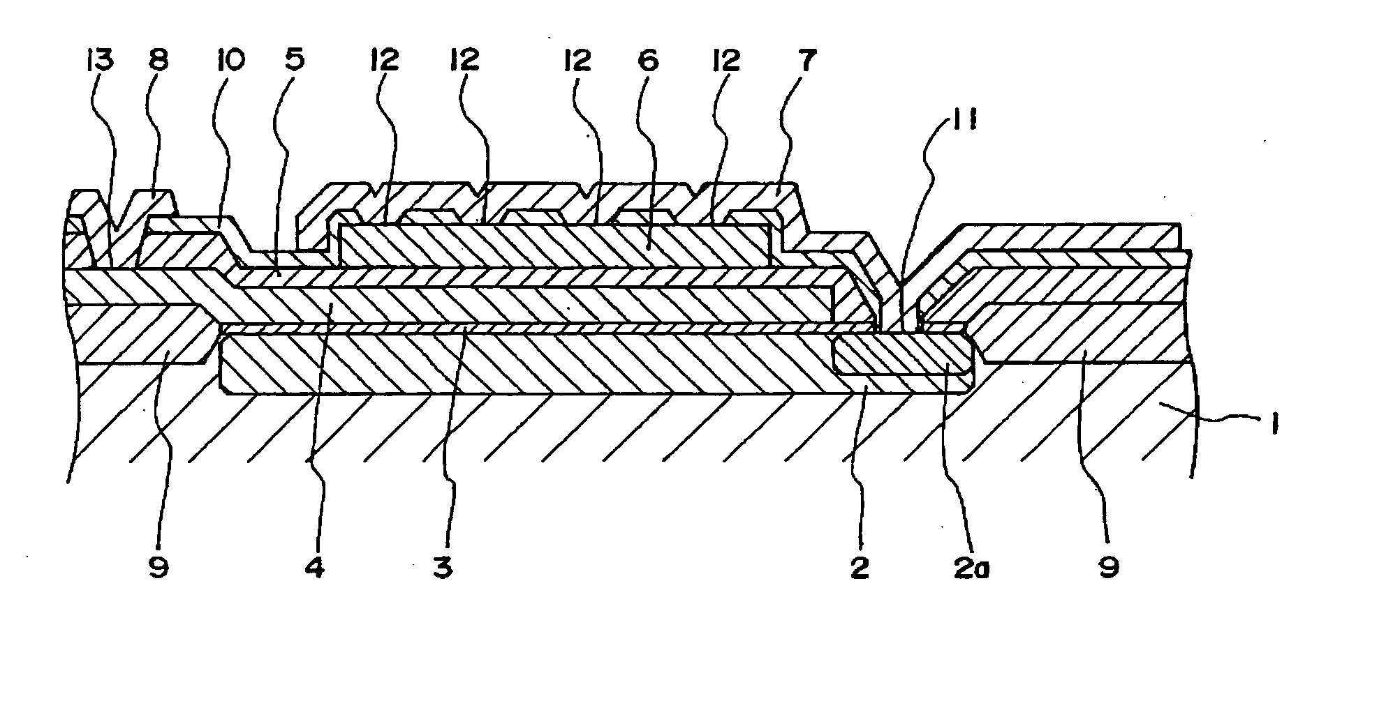
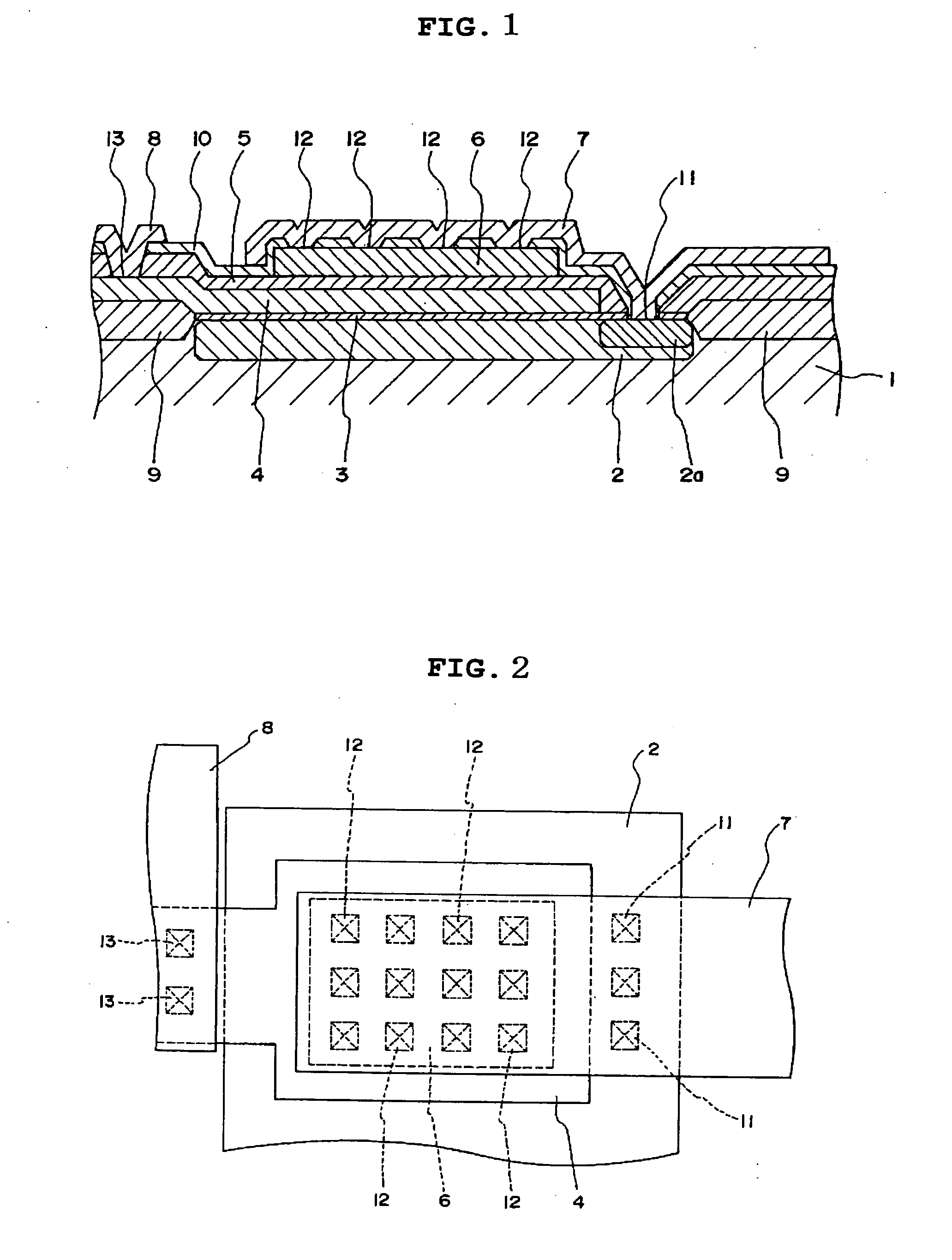
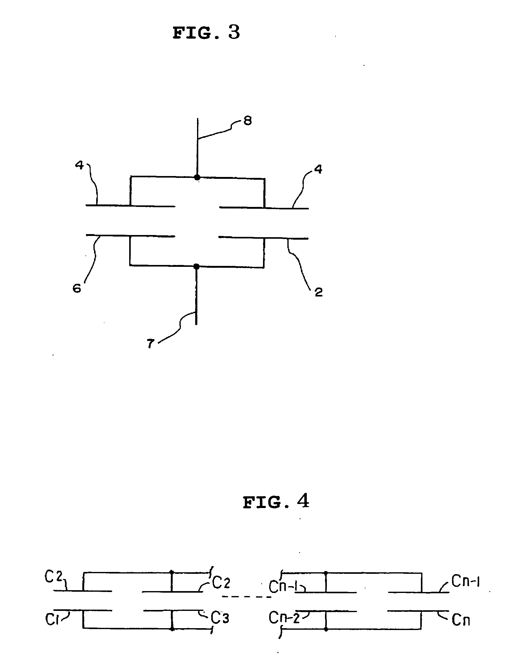
[0015] Now, preferred embodiments of the invention will be described with reference to FIGS. 1 through 3. FIG. 1 is a schematic sectional view of a semiconductor device with a capacitor, FIG. 2 is a plan view thereof, and FIG. 3 is a circuit diagram for explaining the constitution of the capacitor.

[0016] As shown in FIG. 1, on a silicon substrate 1 of a semiconductor device, impurity ions such as arsenic or phosphorus are implanted to form an N-diffusion layer 2 and a diffusion region 2a where the impurity ions are partially implanted at a high concentration. The diffusion layer 2 constitutes an electrically conductive layer, and a first insulating layer 3 comprised, for example, of silicon oxide is formed on and overlies the electrically conductive diffusion layer 2. A lower electrically conductive layer 4, preferably comprised of polysilicon, is formed on and overlies the first insulating layer 3. Thereby, a first capacitor is formed having the first insulating layer 3 as a diele...


PUM


Abstract

A semiconductor device with a capacitor structure for improving area utilization comprises a plurality of electrically conductive layers and a plurality of dielectric layers. The dielectric layers and the electrically conductive layers are alternately superposed one over another, and the electrically conductive layers are alternately electrically connected.

Description

BACKGROUND OF THE INVENTION [0001] 1. Field of the Invention [0002] The invention relates generally to a semiconductor device with a capacitor and, in particular, to the structure of the capacitor. [0003] 2. Description of the Related Art [0004] A capacitor in an existing semiconductor device generally has a structure where, above and below an insulating layer that constitutes a dielectric layer, electrically conductive layers constituting a pair of electrodes are formed. A capacitance value of the capacitor is determined by the dielectric constant of the dielectric layer and the area size of the capacitor. The “area size” means the overlapping facing area of the opposed electrically conductive layers that sandwich the dielectric layer. (See Japanese Unexamined Patent Application Publication No. JP-A-5-190766). SUMMARY OF THE INVENTION [0005] In the prior art capacitor structure, assuming the condition that the dielectric constants are same, in order to increase the capacitance valu...

Claims


Application Information

Patent Timeline
Patent Type & Authority Applications(United States)
IPC IPC(8): H01L21/8242H01L27/108
CPCH01L27/0805H01L28/86H01L28/82
Inventor SAKAMOTO, SHUJI
Owner SEIKO NPC
Why Eureka
Try Eureka