Liquid crystal display

a liquid crystal display and display device technology, applied in semiconductor devices, instruments, optics, etc., can solve the problems of significant decrease in the aperture ratio associated with the footprint of storage capacitors, difficult to reconcile a high aperture ratio and a large capacitance value, and reduce the aperture ratio. , to achieve the effect of large capacitance value and high aperture ratio

Inactive Publication Date: 2009-08-20
SHARP KK
View PDF16 Cites 0 Cited by
  • Summary
  • Abstract
  • Description
  • Claims
  • Application Information

AI Technical Summary

Benefits of technology

[0017]In order to solve the problems described above, preferred embodiments of the present invention provide an active matrix liquid crystal display device which has a high aperture ratio and in which storage capacitors having a sufficiently large capacitance value are provided.

Problems solved by technology

However, since the storage capacitor Cs includes a light-shielding member (i.e., the storage-capacitor counter electrode 518 in the illustrated construction) in its construction, providing a storage capacitor Cs with a large area to obtain an increased capacitance value will result in a decrease in the aperture ratio.
Thus, the capacitance value of a storage capacitor and the aperture ratio have a trade-off relationship, thus making it difficult to reconcile a high aperture ratio and a large capacitance value.
In recent years, liquid crystal display devices are acquiring higher and higher definition, and a decrease in the aperture ratio associated with the footprint of storage capacitors is a significant problem.

Method used


Image

  • Liquid crystal display
  • Liquid crystal display
  • Liquid crystal display

Examples


Embodiment Construction

[0035]Hereinafter, preferred embodiments of the present invention will be described with reference to the drawings. Note that the present invention is not limited to the following preferred embodiments.

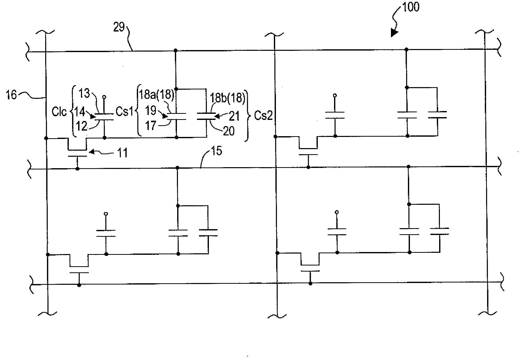
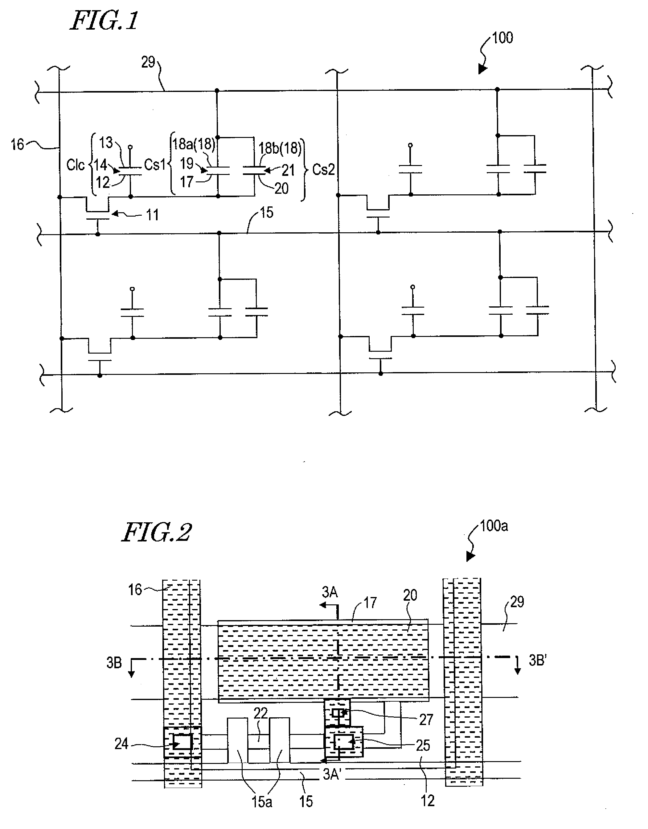
[0036]FIG. 1 schematically shows an equivalent circuit of the liquid crystal display device 100 according to a preferred embodiment of the present invention. As shown in FIG. 1, the liquid crystal display device 100 includes a plurality of pixels which are arranged in a matrix array. In each pixel, a liquid crystal capacitor Clc and a first storage capacitor Cs1 and a second storage capacitor Cs2, which are in parallel electrical connection to the liquid crystal capacitor Clc, are provided.

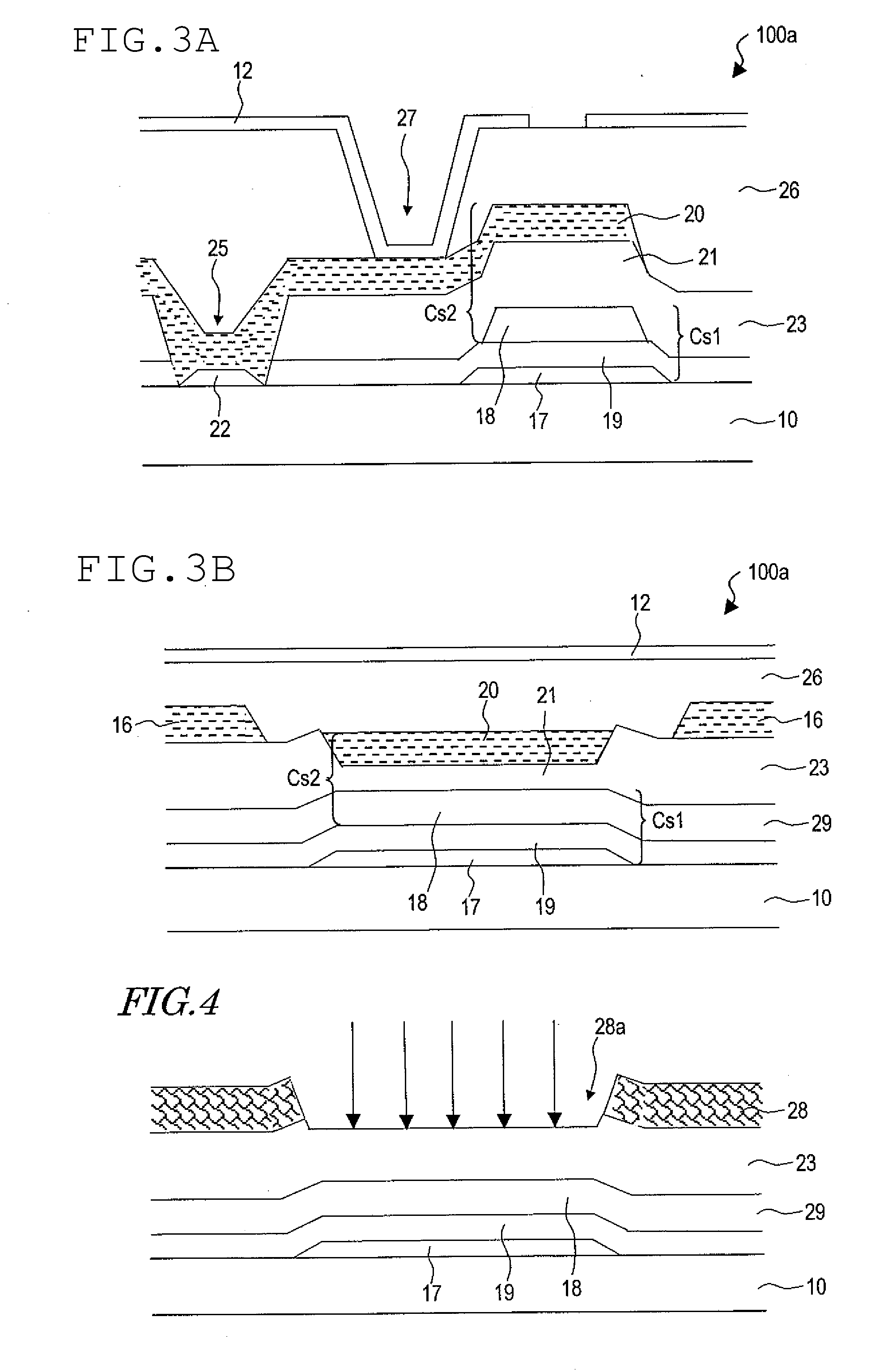
[0037]The liquid crystal capacitor Clc includes: a pixel electrode 12 which is subjected to switching by a thin film transistor 11; a counter electrode 13 opposing the pixel electrode 12; and a liquid crystal layer 14 disposed between the pixel electrode 12 and the counter electrode 13. The thin fil...


PUM

PropertyMeasurementUnit
thickaaaaaaaaaa
insulatingaaaaaaaaaa
semiconductoraaaaaaaaaa

Abstract

A liquid crystal display includes a plurality of pixels arranged in a matrix array, each pixel including a liquid crystal capacitor which includes a pixel electrode subjected to switching by a top-gate type thin film transistor, a counter electrode opposing the pixel electrode, and a liquid crystal layer disposed therebetween, and a first storage capacitor and a second storage capacitor which are in parallel electrical connection to the liquid crystal capacitor. The first storage capacitor includes a first storage capacitor electrode which is electrically connected to the pixel electrode, a first storage-capacitor counter electrode opposing the first storage capacitor electrode, and a first dielectric layer disposed therebetween. The second storage capacitor includes a second storage capacitor electrode which is electrically connected to the pixel electrode, a second storage-capacitor counter electrode opposing the second storage capacitor electrode, and a second dielectric layer disposed therebetween.

Description

BACKGROUND OF THE INVENTION[0001]1. Field of the Invention[0002]The present invention relates to a liquid crystal display device, and in particular to an active matrix liquid crystal display device in which a storage capacitor is provided for each pixel.[0003]2. Description of the Related Art[0004]Liquid crystal display devices are broadly utilized in various fields because of their thinness and low power consumption. In particular, liquid crystal display devices of an active matrix type, including a thin film transistor (referred to as a “TFT”) for each pixel, have a high contrast ratio and excellent response characteristics, and are used in television sets, monitor devices, and laptop computers because of their high performance. The market scale thereof has been increasing in the recent years.[0005]In a traditional active matrix liquid crystal display device, a storage capacitor is provided for each pixel in order to suitably retain a voltage which is applied across a liquid cryst...

Claims


Application Information

Patent Timeline
Patent Type & Authority Applications(United States)
IPC IPC(8): G02F1/1343
CPCG02F1/136213H01L27/1255G02F2001/13685G02F1/136227G02F1/13685
Inventor MORIYA, YOSHIMIZUNAKAJIMA, MUTSUMI
Owner SHARP KK
Why Eureka
Try Eureka