Protection device against electromagnetic interference

Inactive Publication Date: 2012-10-18
ROBERT BOSCH GMBH
View PDF2 Cites 1 Cited by
  • Summary
  • Abstract
  • Description
  • Claims
  • Application Information

AI Technical Summary

Benefits of technology

[0006]It is an object of the invention to provide a protection device with which improved protection in relation to line-conducted interference, in particular at relatively high frequencies, can be obtained and improved adaptation to the required interference immunity of the circuit to be protected can be achieved. Moreover, the abovementioned disadvantages in the case of conventional protective circuitries are intended to be avoided.
[0009]With regard to a compact structural size it is advantageous if the filter structure of the input filter is formed from an area-optimized arrangement composed of capacitive area elements and conductor tracks.
[0011]The minimal space requirement to be striven for can be obtained, in particular, if the dielectric between the electrodes and the grounded conductor layer is formed from a material having high dielectric constants and high dielectric strength and in each case has a layer thickness of less than 150 μm. The use of such particularly thin layers makes possible comparatively large capacitance values. By way of example, ceramic-PTFE composite materials (e.g. Ro3010 from Rogers Corp.) having a relative permittivity εr of about 10 and having very good material properties particularly in the RF range are suitable as the dielectric. Moreover, such a material has a good processability for producing printed circuit boards.
[0014]This optimized arrangement can be modified depending on the material used and the interference immunity of the circuit to be protected relative to the overcoupled portions since the transfer function of the protection circuit is adaptable with regard to a cut-off frequency shift and / or a bandwidth adaptation by means of dimensional adaptation of the capacitance structures, wherein the dimensional adaptation can be carried out by means of a length and / or width adaptation of individual capacitors and / or by means of a scaling of the side length of the entire filter structure. A scaling of the side length of the filter structure to smaller side lengths brings about, for example, an increase in the cut-off frequency, and vice versa, wherein a reduction of the side length by the factor 2 corresponds approximately to a doubling of the cut-off frequency. By means of the length and / or width adaptations of individual capacitors, it is possible to vary specific bandpass filter sections in the transfer function. An optimum adaptation is thus possible in the individual case, which would not be possible for discrete population of a protection circuit on account of the component variation.

Problems solved by technology

Line-conducted interference such as electrostatic discharges (ESD) for example, can couple into electronic assemblies and damage the latter.
They are generally expensive and in some instances have a large space requirement.
The capacitance is dimensioned according to empirical values, although in practice this can often lead to a non-optimum design of the protective circuitry.
Moreover, a certain degradation behavior is observed, i.e. a reduction of the capacitance as a result of repeated pulse loading and associated loss of the blocking capability.
Besides this effect, a parasitic, series inductance can prevent the charge carriers coupling in with the pulse edge from rapidly flowing away, as a result of which the filter properties of the arrangement are impaired.

Method used


Image

  • Protection device against electromagnetic interference
  • Protection device against electromagnetic interference
  • Protection device against electromagnetic interference

Examples


Embodiment Construction

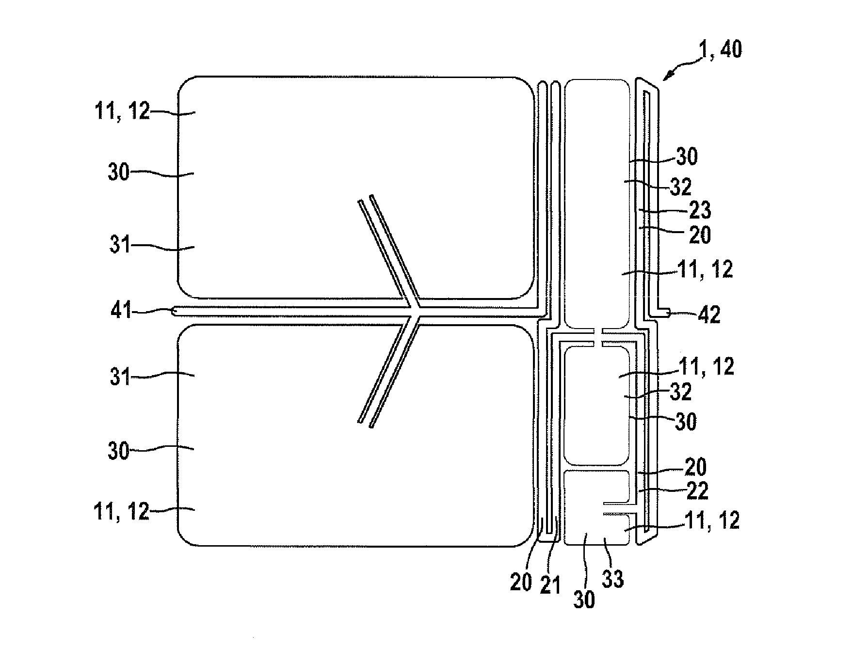
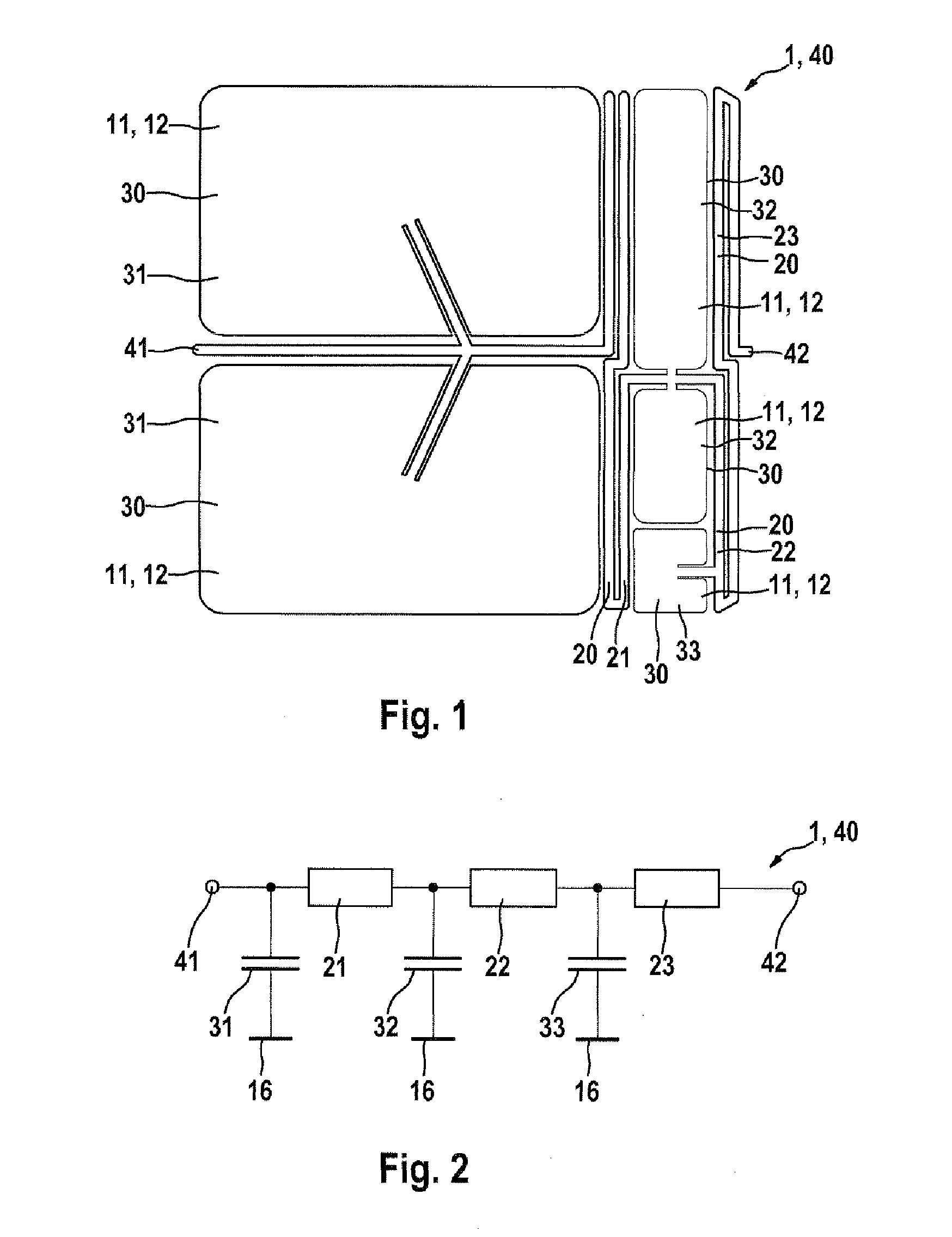
[0022]FIG. 1 illustrates a plan view of a protection device 1 comprising capacitance and induction structures 30, 20, which forms a protection circuit 40, wherein the capacitance structure 30 is illustrated according to the invention as an embedded component in a printed circuit board. In this view, therefore, only the electrodes 11, 12 of the capacitance structures 30 and the conductor tracks which couple the capacitance structures 30 to one another can be discerned. In this case, the conductor tracks form inductance structures 20. This illustration does not illustrate corresponding counterelectrodes or shielding arrangements and insulator or dielectric layers. These are situated as additional layers that are not visible below and / or above the layer shown.

[0023]In the example shown, a first capacitance 31 are illustrated, which is arranged downstream of the input 41 of the protection circuit 40 directly as viewed in the signal direction and assumes a comparatively large value in ac...


PUM


Abstract

The invention relates to a protection device for reducing grid-bound interference, comprising a protection circuit as an input filter of an electronic circuit, wherein the electronic circuit is applied to a multilayer circuit board or is at least partially integrated therein, wherein individual components of the circuit are implemented as embedded structures in the multilayer circuit board. According to the invention, the protection circuit is formed by a cascade of at least as two capacitances coupled to each other by means of low-inductance circuit board structures, wherein the capacitances are implemented as embedded capacitor structures on or within the multilayer circuit board. By means of said protection device, improved filter behavior can be achieved relative to discretely populated protection filters, in particular at higher frequencies, leading to improved protection against electrostatic interference. The filter structure can further be adjusted very well in simulation to the required interference resistance of the circuit to be protected, and also achieve improved aging behavior.

Description

BACKGROUND OF THE INVENTION[0001]The invention relates to a protection device for reducing line-conducted interference, comprising a protection circuit as an input filter of an electronic circuit, wherein the electronic circuit is applied on a multilayer printed circuit board or is at least partly integrated into the latter, wherein individual components of the circuit are embodied as embedded structures in the multilayer printed circuit board.[0002]Line-conducted interference such as electrostatic discharges (ESD) for example, can couple into electronic assemblies and damage the latter. In order to protect these circuits, so-called blocking structures are used, which are usually constructed from discrete components.[0003]Examples thereof are varistors, voltage-dependent resistors, or spark gaps which are arranged at the start of the coupling-in path of the circuit to be protected. They are generally expensive and in some instances have a large space requirement. Furthermore, SMD ca...

Claims


Application Information

Patent Timeline
IPC IPC(8): H02H9/00
CPCH05K1/0231H05K1/0233H05K2201/09263H05K1/165H05K1/162
Inventor SPRATLER, CHRISTIAN
Owner ROBERT BOSCH GMBH
Why Eureka
Try Eureka