

Semiconductor device and method of manufacturing the same
a technology of semiconductor devices and semiconductors, applied in the direction of semiconductor devices, basic electric elements, electrical equipment, etc., can solve the problems of not easy to break the bond between a silicon atom and a nitrogen atom, and the bond between a silicon atom and an on-group is not easy to break, so as to improve the performance of the transistor
- Summary
- Abstract
- Description
- Claims
- Application Information
AI Technical Summary
Benefits of technology
Problems solved by technology
Method used
Image

Examples
Embodiment Construction
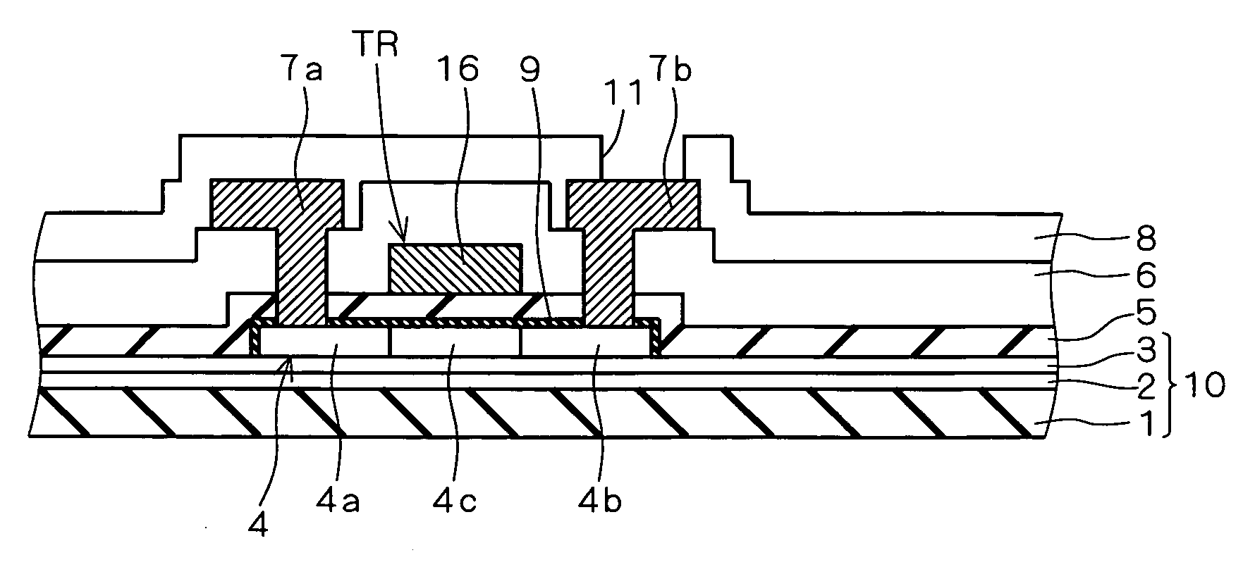
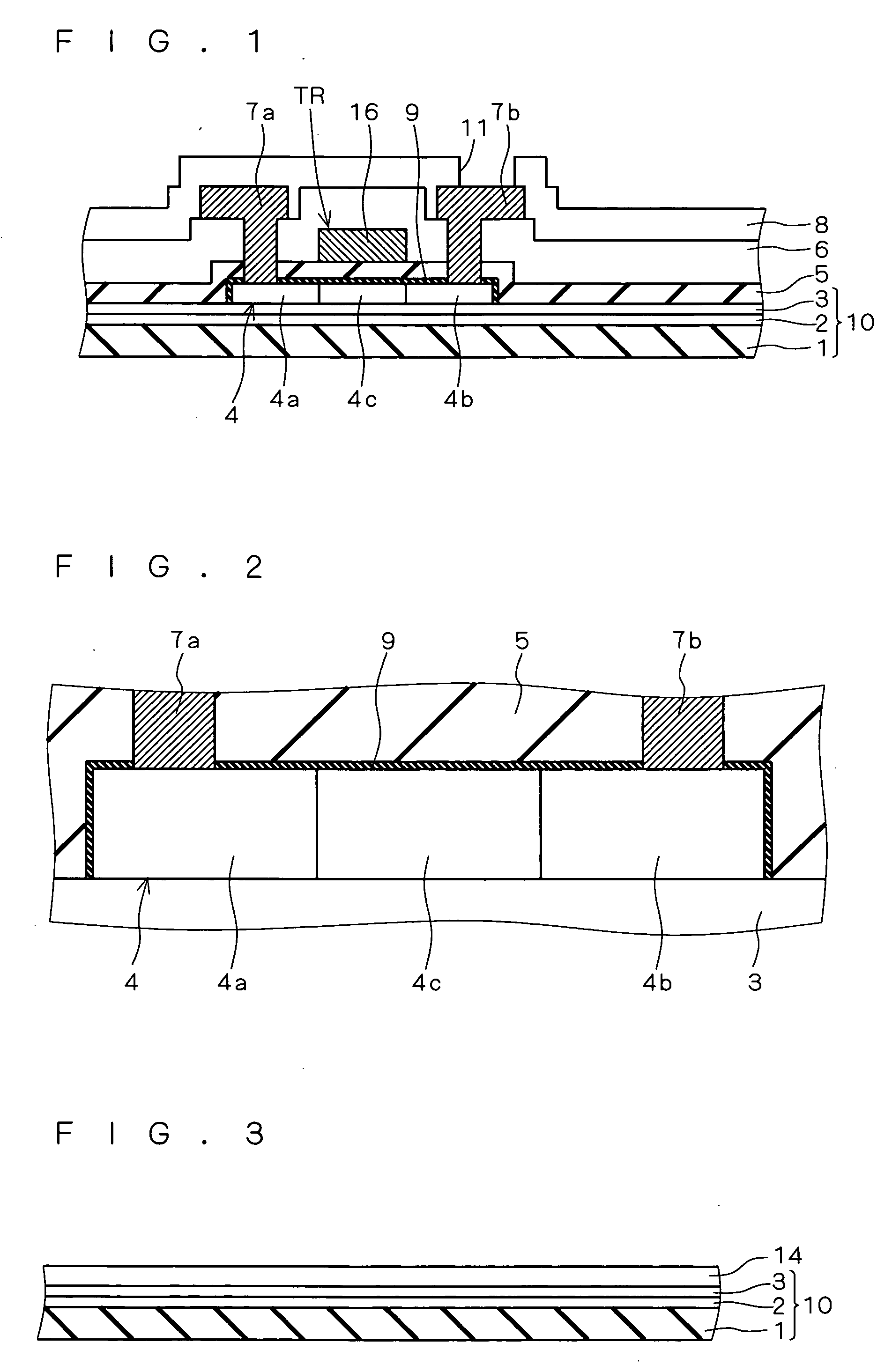
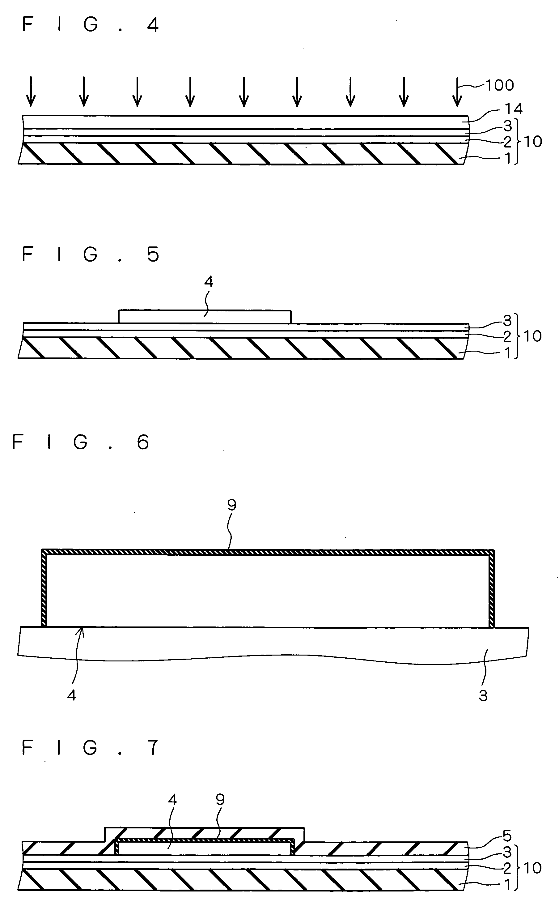
[0022]FIG. 1 is a sectional view of a structure of a semiconductor device according to one preferred embodiment of the present invention. FIG. 2 is an enlarged sectional view of a portion of the structure of the semiconductor device according to the preferred embodiment of the present invention. The semiconductor device according to the preferred embodiment of the present invention is used as a drive circuit incorporated in a liquid crystal panel, for example, and includes an n-type thin-film transistor TR serving as a switching element.
[0023] As illustrated in FIG. 1, the semiconductor device according to the preferred embodiment of the present invention includes an insulating layer 10. The insulating layer 10 includes an insulating substrate 1 including a glass substrate, for example, an insulating film 2 formed on the insulating substrate 1, and an insulating film 3 formed on the insulating film 2. Each of the insulating films 2 and 3 is light permeable. The insulating films 2 a...
PUM
 Abstract
Description
Claims
Application Information