Electronic part mounting method, semiconductor module, and semiconductor device

a technology for semiconductor modules and electronic parts, applied in the direction of printed circuit aspects, sustainable manufacturing/processing, final product manufacturing, etc., can solve the problems of difficult hierarchical setting of bonding temperatures for semiconductor modules, further reduction of thickness, and reduced height of semiconductor modules, so as to reduce the thickness of the device and the mounting area.

Inactive Publication Date: 2006-11-30
HITACHI LTD
View PDF8 Cites 46 Cited by
  • Summary
  • Abstract
  • Description
  • Claims
  • Application Information

AI Technical Summary

Benefits of technology

[0038] Thus, the present invention can provide the electronic part mounting method, the semiconductor module, and the semiconductor device, which can reduce a mounting area and a device thickness.
[0039] Also, the present invention can provide the electronic part mounting method, the semiconductor module, and the semiconductor device, which will not impair reliability for a long term even under environment at high temperatures.

Problems solved by technology

Also, bonding wires for connecting the active parts and the external wiring to each other hinder a reduction of the height of the semiconductor module and hence a further reduction of the thickness.
It is therefore difficult to set the bonding temperatures for them in a hierarchical way.

Method used


Image

  • Electronic part mounting method, semiconductor module, and semiconductor device
  • Electronic part mounting method, semiconductor module, and semiconductor device
  • Electronic part mounting method, semiconductor module, and semiconductor device

Examples


first embodiment

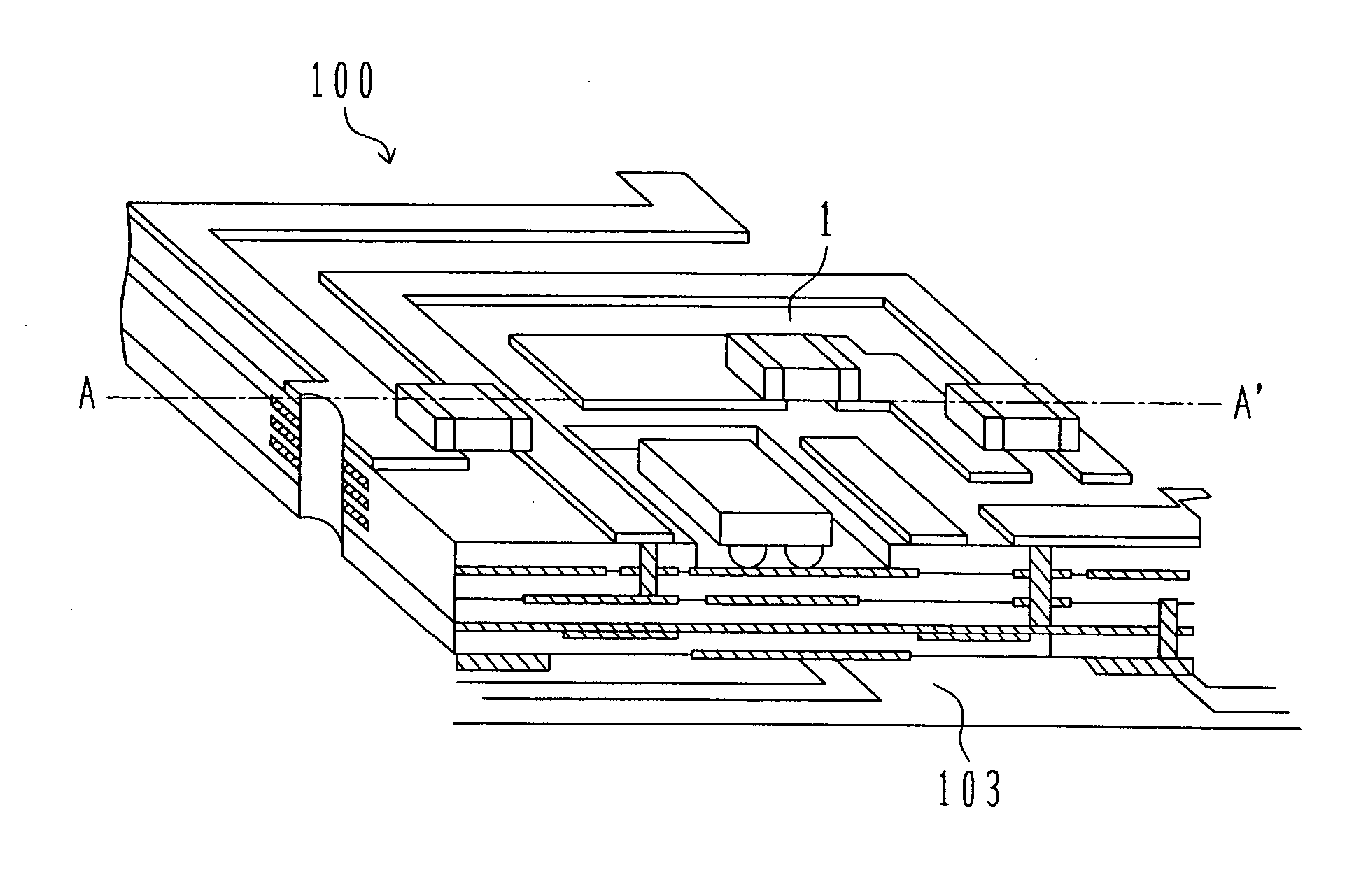
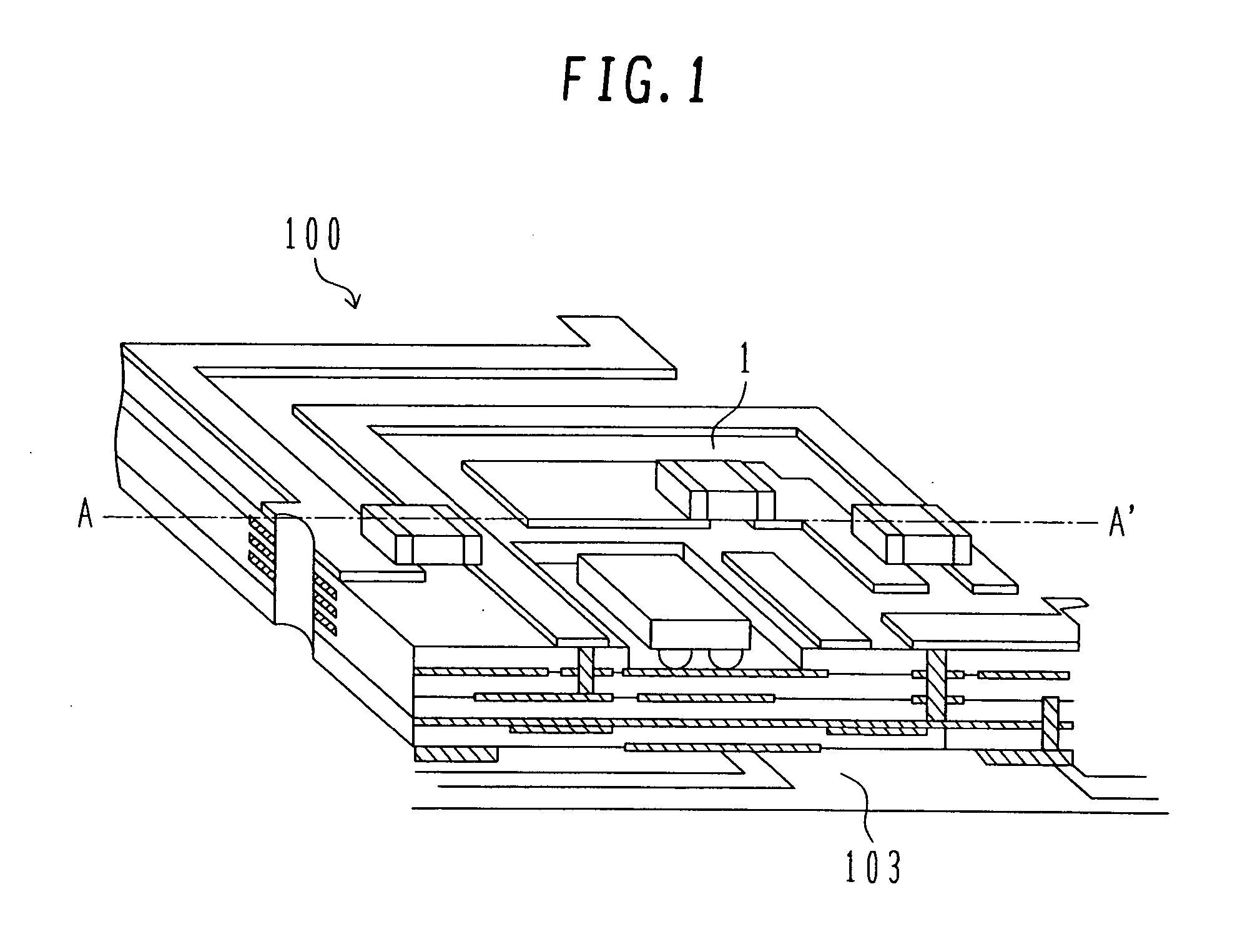
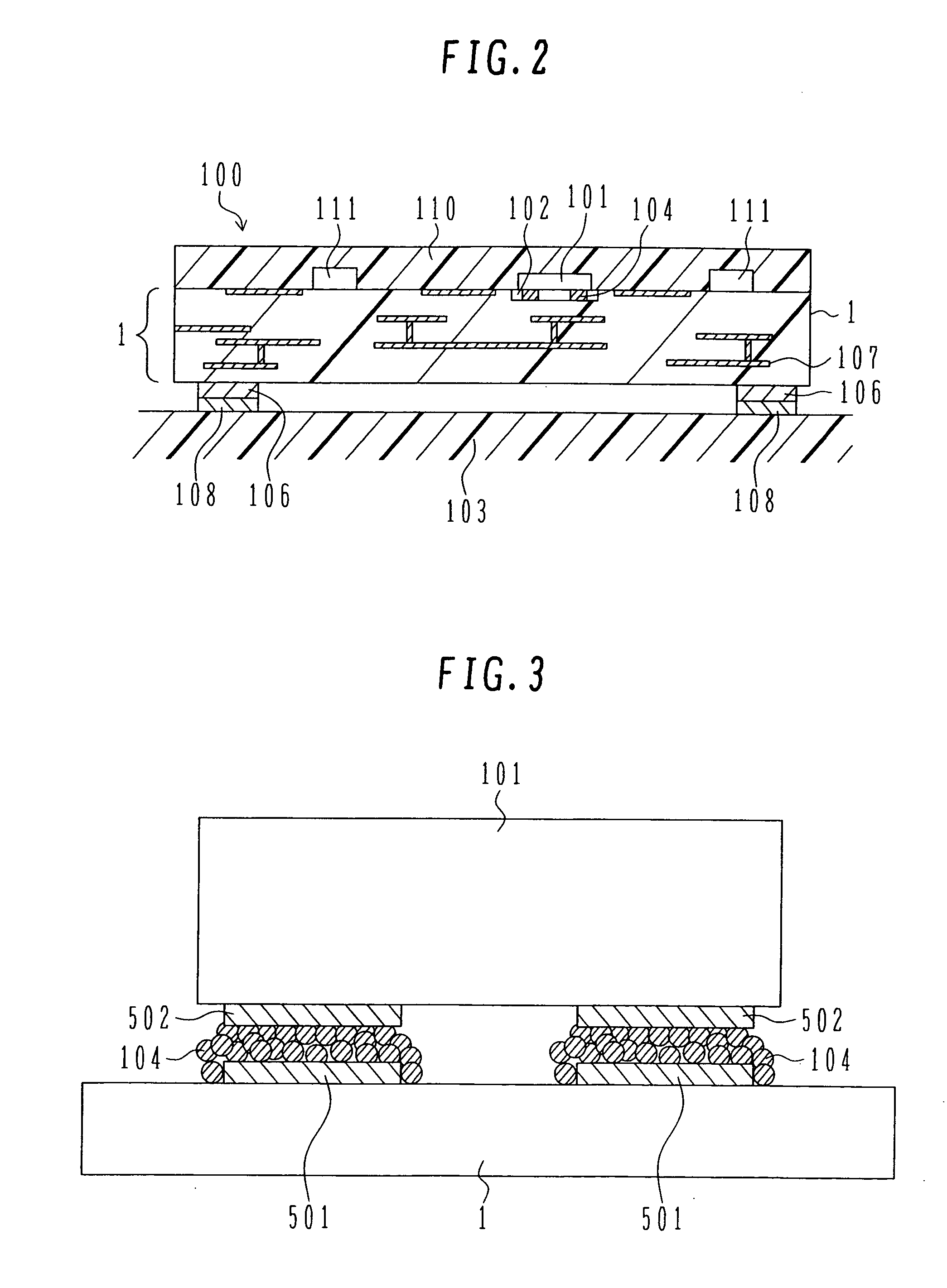
[0063]FIG. 1 is a schematic view showing the construction of a semiconductor module 100 according to one embodiment of the present invention, and FIG. 2 is a vertical sectional view taken along a line A-A′ in FIG. 1. The semiconductor module 100 of this embodiment has a thickness of about 0.45 mm.

[0064] Referring to FIGS. 1 and 2, a glass-ceramic substrate 1 is of a multilayered structure in which patterned wires 107 for transmission are formed between multiple layers and passive parts 111, such as capacitors, resistances and inductors, are formed on the substrate. Also, the substrate 1 has a recess 102 in which a MOSFET device 101 (hereinafter referred to simply as the “MOSFET”) made of a semiconductor material is to be mounted.

[0065] The substrate 1 is mounted on a circuit board 103. Au bumps 104 are used for electrical connection between the MOSFET 101 and the substrate 1, and are each made up of Au particles having an average particle size of 5 nm. Electrodes 108 are formed on...

second embodiment

[0091] A method of manufacturing the semiconductor module of this second embodiment will be described with reference to FIGS. 1 and 2.

[0092] The glass-ceramic substrate 1 (with a thickness of 0.30 mm) of the multilayered structure including the patterned wires for transmission and the passive parts formed therein is prepared by sintering. The recess 102 having a size sufficient to allow mounting of the MOSFET 101 therein is formed in the glass-ceramic substrate 1 at the same time when the glass-ceramic substrate 1 is processed.

[0093] The depth of the recess 102 is set such that a rear surface of the MOSFET 101 is flush with the surface of the glass-ceramic substrate 1 on the MOSFET mounting side. Metallic patterned wires are formed on a MOSFET mounting surface in the recess 102 and have surfaces plated with Au. On the surface of the glass-ceramic substrate 1 on which the passive parts 111, such as capacitors, solenoids and resistances, are to be mounted, there are formed electrode...

third embodiment

[0101] In this third embodiment, the Au bumps used in the first and second embodiments are replaced with Ag bumps. The embodiments described above are each applicable to manufacturing of a high-frequency power amplifier that is used in a transmitting unit of a cellular cell, etc.

[0102]FIG. 8 is a circuit block diagram of a cellular phone in which the semiconductor module according to the embodiment is employed. A voice input signal inputted from a microphone 10 is superimposed in a mixer 12 on a high-frequency signal from an oscillator 14, and then transmitted as an electric wave from an antenna 20 through an insulation semiconductor device (MOSFET) 16, which serves as a power amplifier, and an antenna sharing unit 18.

[0103] Transmission power is monitored by a coupler 22 and the monitored power is fed back to the insulation semiconductor device 16, which serves as a power amplifier, so that the transmission power is kept constant. Electric waves in a band of 800 to 1000 MHz are u...


PUM

PropertyMeasurementUnit
particle sizeaaaaaaaaaa
thicknessaaaaaaaaaa
particle sizeaaaaaaaaaa

Abstract

An electronic part mounting method, a semiconductor module, and a semiconductor device, which can reduce a mounting area and a device thickness. In an electronic part mounting method for bonding an electrode formed on a substrate and an electrode formed on an electronic part to each other, the method comprises the step of bonding both the electrodes through a metal layer made up of aggregated particles of at least one kind of metal. Then, the metal particles have an average particle size of 1 to 50 nm. Preferably, the metal particles form a metal layer having a thickness of 5 to 100 μm.

Description

BACKGROUND OF THE INVENTION [0001] 1. Field of the Invention [0002] The present invention relates to an electronic part mounting method, a semiconductor module, and a semiconductor device. [0003] 2. Description of the Related Art [0004] Usually, a high-frequency power amplifier is incorporated in a portable communication unit represented by a car phone or a cellular phone based on the PDC (Personal Digital Cellular) system, or a cellular phone based on the PHS (Personal Handy-phone System). As well known, the high-frequency power amplifier is constituted as a semiconductor module, and it is a multistage amplifier comprising a plurality of amplifiers interconnected in multiple stages. [0005] Such a high-frequency power amplifier is formed on one principal surface of a semiconductor chip, and the semiconductor chip including the amplifier is mounted on one principal surface of a wiring board. Electrodes formed on the one principal surface of the semiconductor chip and electrodes forme...

Claims


Application Information

Patent Timeline
Patent Type & Authority Applications(United States)
IPC IPC(8): H01L23/48
CPCH01L23/24H01L23/66H01L24/11H01L24/13H01L24/16H01L24/29H01L24/32H01L24/33H01L24/40H01L24/41H01L24/81H01L24/83H01L25/072H01L25/16H01L2223/6644H01L2224/11505H01L2224/13099H01L2224/13139H01L2224/13144H01L2224/16225H01L2224/27505H01L2224/32225H01L2224/48091H01L2224/48227H01L2224/48472H01L2224/49111H01L2224/49175H01L2224/73265H01L2224/81191H01L2224/81192H01L2224/8121H01L2224/81815H01L2224/83191H01L2224/83192H01L2224/83801H01L2224/8384H01L2924/01005H01L2924/01013H01L2924/01022H01L2924/01027H01L2924/01029H01L2924/0103H01L2924/01033H01L2924/01042H01L2924/01046H01L2924/01047H01L2924/01049H01L2924/0105H01L2924/01061H01L2924/01073H01L2924/01074H01L2924/01077H01L2924/01078H01L2924/01079H01L2924/01082H01L2924/01322H01L2924/09701H01L2924/10272H01L2924/12044H01L2924/13055H01L2924/13091H01L2924/14H01L2924/15153H01L2924/1517H01L2924/19041H01L2924/19042H01L2924/19043H01L2924/19105H05K1/183H05K3/102H05K3/321H05K3/328H05K2201/0218H05K2201/0257H05K2201/10636H05K2201/10674H05K2203/1131H01L24/48H01L24/49H01L2224/29H01L2224/2919H01L2924/01006H01L2924/01019H01L2924/01023H01L2924/01024H01L2924/01044H01L2924/01045H01L2924/01072H01L2924/01076H01L2924/014H01L2924/0665H01L2224/29101H01L2924/0132H01L2924/0133H01L2224/29111H01L2224/45124H01L2224/45147H01L2924/15787H01L2924/15788H01L2224/29144H01L2924/00013H01L2224/29344H01L2924/19107H01L2924/10253H01L2924/12041H01L2224/11332H01L2924/1306H01L2924/1301H01L2924/00014H01L2924/00H01L2924/01014H01L2924/00015H01L2224/29099H01L2224/29199H01L2224/29299H01L2224/2929H01L2224/45015H01L2924/351H01L2224/40095H01L2224/81205H01L2224/85205H01L2924/00011H01L2224/40225H01L24/45H01L2924/181H01L2224/05573H01L2224/05568H01L2224/05644H01L2224/371H01L24/37H01L2224/0554H01L2224/3754H01L2224/84801H01L2224/8484H01L24/84H01L24/03H01L2224/13339H01L2224/13344H01L2224/13355H01L2224/13439H01L2224/13444H01L2224/13455H01L2224/13347H01L2224/16238H01L2224/13006H01L2224/16013H01L24/05Y02P70/50H01L2224/73221H01L2924/2076H01L2224/83205H01L2924/00012H01L2924/01028H01L2224/05599H01L2224/0555H01L2224/0556H01L2924/013
Inventor HOZOJI, HIROSHIMORITA, TOSHIAKISASAKI, HIROSHI
Owner HITACHI LTD
Why Eureka
Try Eureka