Liquid crystal display device with tablet function

a technology of liquid crystal display device and tablet, which is applied in the direction of user-computer interaction input/output, instruments, computing, etc., can solve the problems of affecting the use of tablet pc as a whol

Inactive Publication Date: 2006-11-30
NEC LCD TECH CORP
View PDF1 Cites 33 Cited by
  • Summary
  • Abstract
  • Description
  • Claims
  • Application Information

AI Technical Summary

Benefits of technology

[0033] With the above configurations, coordinate position detecting devices each formed in a manner to correspond to at least part of the pixel electrodes, when receiving light emitted from a position designating unit that inputs a coordinate position by designation using light, output coordinate po...

Problems solved by technology

Such the conventional tablet PC has problems.
That is, since layers of tablets are deposited on a display screen, a display screen is visually recognized as if the display screen has lain deep therein, causing the display screen to become hard to view (due to a “deep window effect”) and also causing the tablet PC to be thick and heavy as a whole.
A problem to be solved in the above conventional technologies is that the light detecting devices are put into an ON state in error in some cases.
There are some cases in which, when a phototransistor is used as a light detecting device, the light detecting device is put into the ON state in error, even without irradiation with light from a light pen or a like, due to leaked light from, for example, a backlight.
That is, when a bipolar phototransistor is used as a light detecting device, due to use of the phototransistor having a pnp or npn structure with its base being in a floating state, if a potential difference between both terminals (between an emitter and collector) is large, the light detecting device is put into an ON state in error by an effect of a...

Method used


Image

  • Liquid crystal display device with tablet function
  • Liquid crystal display device with tablet function
  • Liquid crystal display device with tablet function

Examples


first embodiment

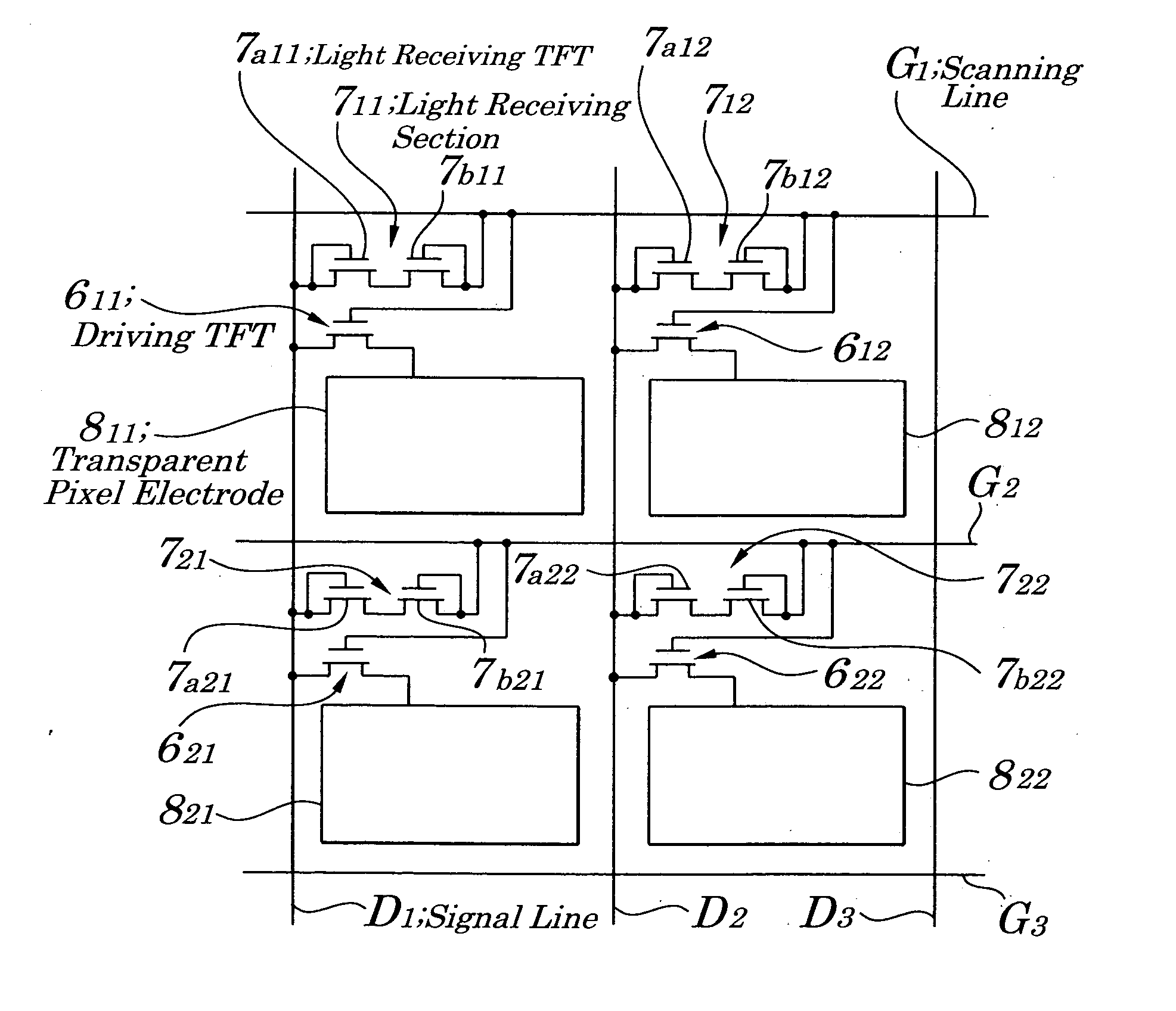
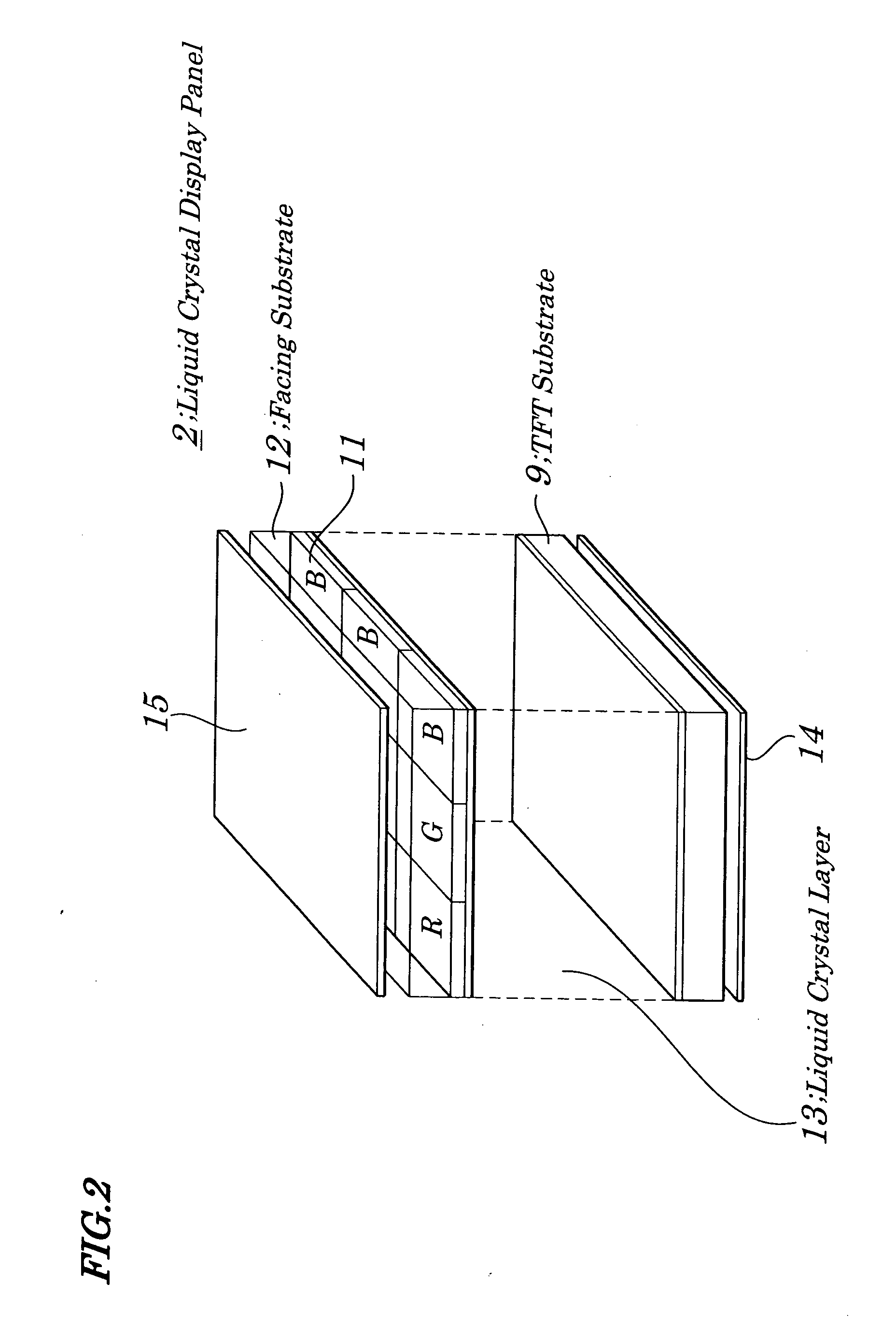
[0046]FIG. 1 is an equivalent circuit diagram showing electrical configurations of a liquid crystal panel of the first embodiment of the present invention. FIG. 2 is a perspective view schematically showing configurations of the liquid crystal panel of FIG. 1. FIG. 3 is a cross-sectional view schematically showing configurations of the liquid crystal panel of FIG. 1. FIG. 4 is a schematic block diagram showing electrical configurations of a liquid crystal display device using the liquid crystal display panel of FIG. 1. FIG. 5 is a plan view showing configurations of a TFT substrate used in the liquid crystal display panel of FIG. 1. FIG. 6 is a cross-sectional view of the liquid crystal panel of FIG. 1 taken from a line A-A in FIG. 5.

[0047] The liquid crystal display device 1 of the first embodiment is used, for example, as an inputting device or displaying device for a tablet PC and includes, as shown in FIGS. 2 to 4, a liquid crystal display panel 2, an LCD (Liquid Crystal Displa...

second embodiment

[0070]FIG. 7 is an equivalent circuit diagram showing electrical configurations of a liquid crystal panel of the second embodiment of the present invention. FIG. 8 is a plan view showing configurations of TFTs of the liquid crystal display panel of FIG. 7. FIG. 9 is a cross-sectional view of the liquid crystal panel of FIG. 7 taken from a line B-B in FIG. 8. Configurations of the second embodiment differ greatly from those of the first embodiment in that its light receiving section is made up of a pair of light receiving TFTs in which gate electrodes are connected to each other. Other configurations other than above are approximately the same as those in the first embodiment described above and their descriptions are omitted accordingly.

[0071] In the second embodiment, on the TFT substrate 41 are formed a plurality of transparent pixel electrodes 4211, 4212, . . . , in a matrix form and, in an area surrounding each of the plurality of transparent pixel electrodes 4211, 4212, . . . ...

third embodiment

[0077]FIG. 10 is an equivalent circuit diagram showing electrical configurations of a liquid crystal panel of the third embodiment of the present invention. Configurations of the third embodiment differ greatly from those of the first embodiment in that each of light receiving section TFTs is made up of a single light receiving TFT and each of the light receiving TFTs is connected to signal lines and to each of light detecting wirings provided in parallel to the scanning lines, instead of the scanning lines used in the first and second embodiments. Configurations other than above are approximately the same as those in the first embodiment described above and their descriptions are omitted accordingly.

[0078] As shown in FIG. 10, on the TFT substrate 41 of the embodiment are formed a plurality of transparent pixel electrodes 611, 6112, . . . , in a matrix form and, in an area surrounding each of the plurality of transparent pixel electrodes 6111, 6112, . . . , are provided each of th...


PUM


Abstract

A liquid crystal display device having a tablet function is provided which is capable of reliably preventing malfunction. Light receiving devices are made up of TFTs (Thin Film Transistors) having approximately the same structure as driving switching elements. A semiconductor layer making up the light receiving devices, in particular, is made up of a non-doped a-Si (amorphous silicon) layer and a doped n+-type a-Si layer. A gate electrode of each of light receiving TFTs is connected to its own source electrode and to its own drain electrode. This prevents each of the light receiving TFTs from being put, in error, into an ON state. The light receiving TFTs can be kept reliably in an OFF state irrespective of setting of a bias level, which prevents reliably malfunction. By detecting optical currents generated in the light receiving devices, light input positions can be identified accurately and reliably.

Description

BACKGROUND OF THE INVENTION [0001] 1. Field of the Invention [0002] The present invention relates to a liquid crystal display device having a tablet function and more particularly to the liquid crystal display device with the tablet function in which a plurality of light detecting devices to receive outgoing light from a light pen or a like and to detect a position shown by coordinates input by designating the position are formed on a substrate on which pixel electrodes and switching elements are arranged in a matrix form. [0003] The present application claims priority of Japanese Patent Application No. 2005-158215 filed on May 30, 2005, which is hereby incorporated by reference. [0004] 2. Description of the Related Art [0005] Conventionally, an information processing device called a “tablet PC (Personal Computer)” in which layers of tablets allowing a position to be input by detecting pressure are deposited on a surface of a liquid crystal panel is being widely used. The convention...

Claims


Application Information

Patent Timeline
IPC IPC(8): G02F1/1335G09G5/00
CPCG02F1/13338G06F3/0412G02F1/13624G06F3/042
Inventor TAKAHASHI, MITSUASA
Owner NEC LCD TECH CORP
Why Eureka
Try Eureka