Nanotube-organic photoelectric conversion device and methods of making same

a conversion device and organic technology, applied in the field of organic organic photoelectric conversion devices, can solve the problems of large volume of panels, limited general use, and inability to meet the requirements of the application

Inactive Publication Date: 2006-12-07
RENESSELAER POLYTECHNIC INST
View PDF20 Cites 109 Cited by
  • Summary
  • Abstract
  • Description
  • Claims
  • Application Information

AI Technical Summary

Problems solved by technology

While reasonable efficiencies have been achieved (10-20%), they are still limited in general use due to the prohibitive costs.
However, the inhibiting factor is still costs and applicability.
What is meant by applicability is that most panels are large and unwieldy, considering the amount of power generated.
It is difficult to produce panels that can be applied to any surface, such as curved, ceramic, metallic or plastic.
Hence this morphology problem exacerbates the problem.
Progress towards producing polymeric materials in a robust opto-electronic fashion creates a host of problems which include sensitivity to intensity (power) within the polymer, long term instabilities due to photo-chemical effects, low thermal and electrical conductivity (necessary for transport related functions), and relatively low third order effects.

Method used


Image

  • Nanotube-organic photoelectric conversion device and methods of making same
  • Nanotube-organic photoelectric conversion device and methods of making same
  • Nanotube-organic photoelectric conversion device and methods of making same

Examples


first embodiment

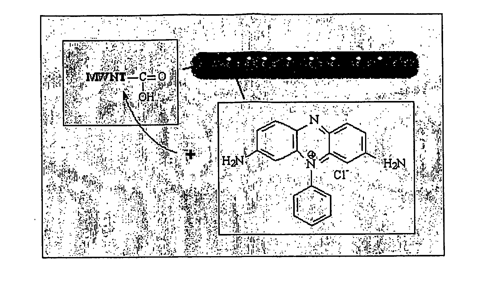
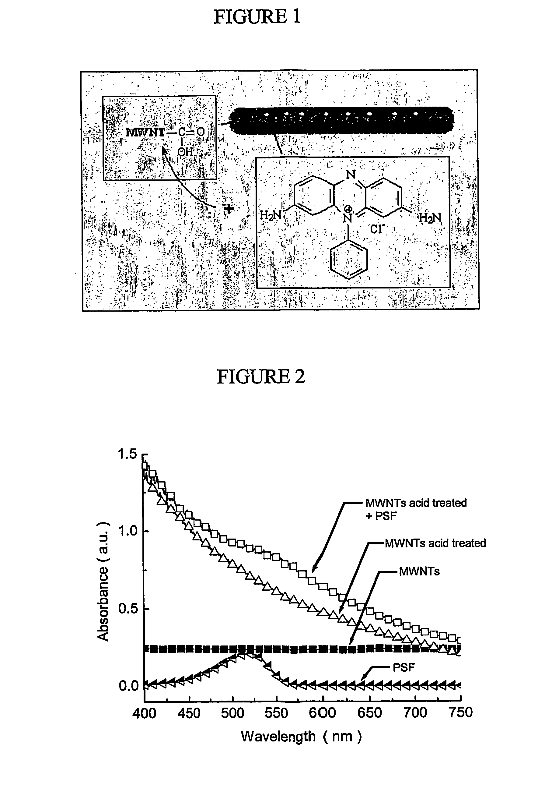
[0022] In a preferred aspect of the first embodiment, a cationic phenazine dye, phenosafranin (PSF), is used. However, any other suitable dye may be attached to the nanotubes in a similar fashion. PSF is advantageous because phenazine dyes have great potential for use in solar cells. For example, PSF coupled with EDTA generates photovoltages of about 600 mV. In addition, PSF can undergo reversible reduction with long-lived excited states which make it a good photosensitizer in energy and electron transfer reactions. The amine functionalities make PSF suitable for dispersion in Nylon 6 or other similar polymer matrices, since the amine functionalities may be incorporated into Nylon 6 polymer backbone.

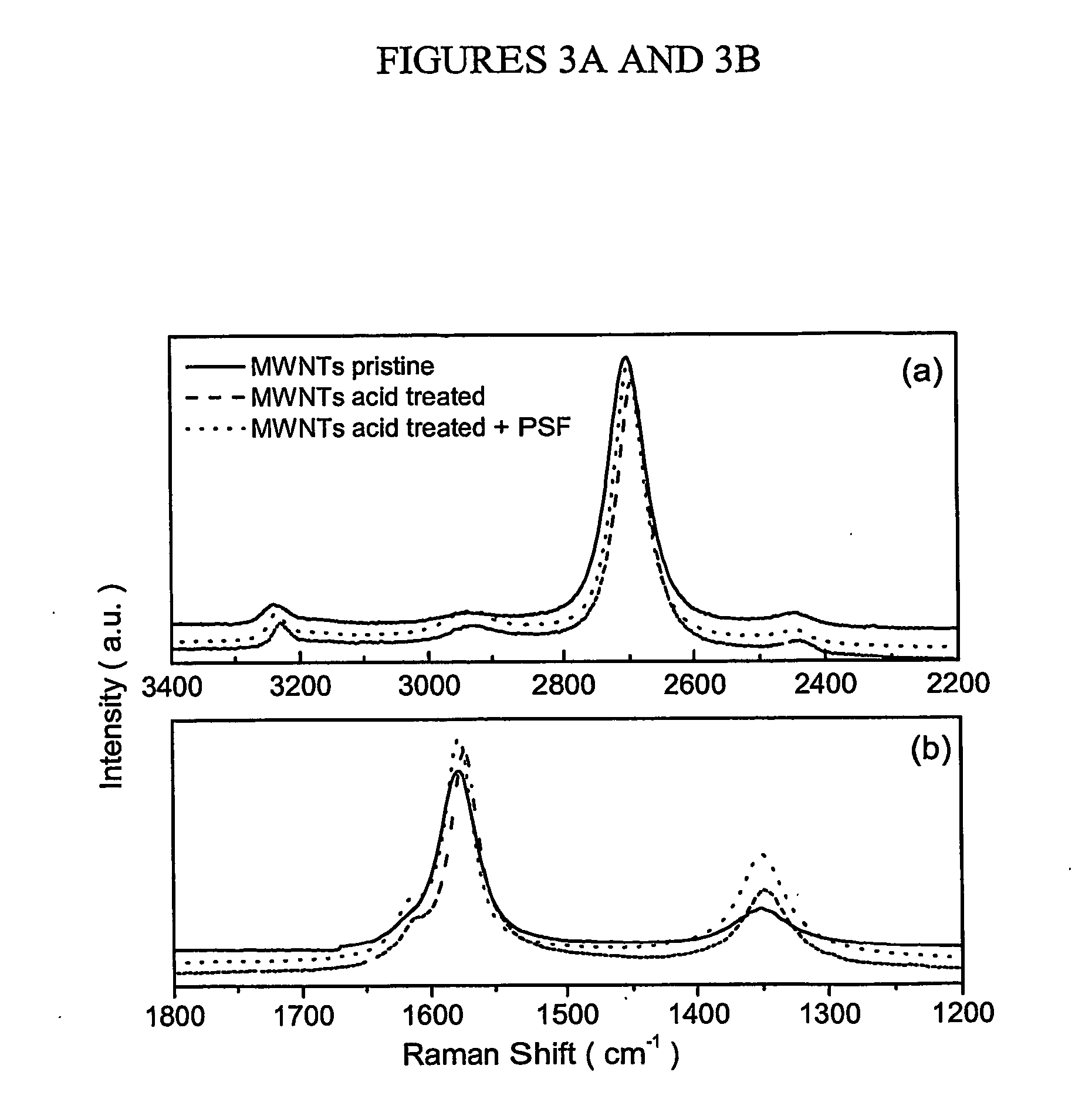
[0023] The following specific but non-limiting example of the method of the first embodiment is presented for illustration of the method. MWNTs synthesized by the arc-discharge method were first purified by sonication in concentrated 70 / 30 H2SO4 / HNO3 in an ultrasonic bath for 6 hours. Ot...

second embodiment

[0031] The anionic process of the invention involves the use of an ionizing agent or anionic initiator. An anionic initiator is any agent which can add to double bonds on the nanotube surface thereby generating anions (carbanions) on the surface of the nanotubes. Anionic initiators include, for example, metal organic initiators such as alkyl lithium compounds (salts), such as sec-butyllithium, as well as other alkali metal organic compounds, such as fluorenyl-sodium and cumyl-sodium. Radical ionic initiators such as sodium naphthalenide may also be used.

[0032] In one aspect of the second embodiment, anions that are formed on the surface of the nanotubes using the anionic process are subsequently quenched (i.e., protonated) with an alcohol (e.g., methanol or ethanol). The resulting nanotubes may be considered to be derivatized by virtue of the fact that the ionizing agent which has added to the nanotube double bond is still attached. When the anionic initiator used is an alkyl lithiu...


PUM

PropertyMeasurementUnit
photovoltagesaaaaaaaaaa
lengthaaaaaaaaaa
organicaaaaaaaaaa

Abstract

An organic photovoltaic conversion device, such as a solar cell includes a matrix material, such as a polymer matrix material, carbon nanotubes dispersed in the matrix material, and photovoltaic organic molecules, such as organic dye molecules, attached to defect sites on the carbon nanotubes.

Description

CROSS-REFERENCE TO RELATED APPLICATIONS [0001] This application claims priority to U.S. Provisional Application Ser. No. 60 / 431,948, filed Dec. 9, 2002, the disclosure of which is incorporated by reference herein in its entirety.FIELD OF THE INVENTION [0002] The present invention is directed to nanotube-organic photoelectric conversion devices, such as solar cells, and methods of making thereof. BACKGROUND OF THE INVENTION [0003] Carbon nanotubes (CNTs) are self-assembled coaxial cylindrical graphene sheets of sp2 hybridized carbon atoms. There are two types of CNTs, multi-walled carbon nanotubes (MWNT) and single-walled carbon nanotubes (SWNT). [0004] In recent years, much interest has focused on energy consumption where alternative sources of power have been examined. Currently, most solar panels are made from silicon (monocrystalline, polycrystalline and amorphous states) in large flat panels. While reasonable efficiencies have been achieved (10-20%), they are still limited in ge...

Claims


Application Information

Patent Timeline
Patent Type & Authority Applications(United States)
IPC IPC(8): H01L31/00H01L31/0256H01L51/00H01L51/30H01M
CPCB82Y10/00H01L51/0012H01L51/0049H01L51/0071Y02E10/549H01L51/4206H01L51/424H01L51/4253H01L51/4266H01L51/0072H10K71/191H10K85/225H10K85/657H10K85/6572H10K30/451H10K30/20H10K30/352H10K30/30
Inventor AJAYAN, PULICKELELLIS, AMANDARYU, CHANG Y.CURRAN, SEAMUS
Owner RENESSELAER POLYTECHNIC INST
Why Eureka
Try Eureka