Method for making a semiconductor device including a dopant blocking superlattice

Inactive Publication Date: 2006-12-07
MEARS TECH
View PDF50 Cites 58 Cited by
  • Summary
  • Abstract
  • Description
  • Claims
  • Application Information

AI Technical Summary

Benefits of technology

[0012] In view of the foregoing background, it is therefore an object of the present invention to provide a method for makin

Problems solved by technology

Moreover, as device sizes decrease regions within devices become closer together and dopant diffusion between regions can become problemati

Method used


Image

  • Method for making a semiconductor device including a dopant blocking superlattice
  • Method for making a semiconductor device including a dopant blocking superlattice
  • Method for making a semiconductor device including a dopant blocking superlattice

Examples


Embodiment Construction

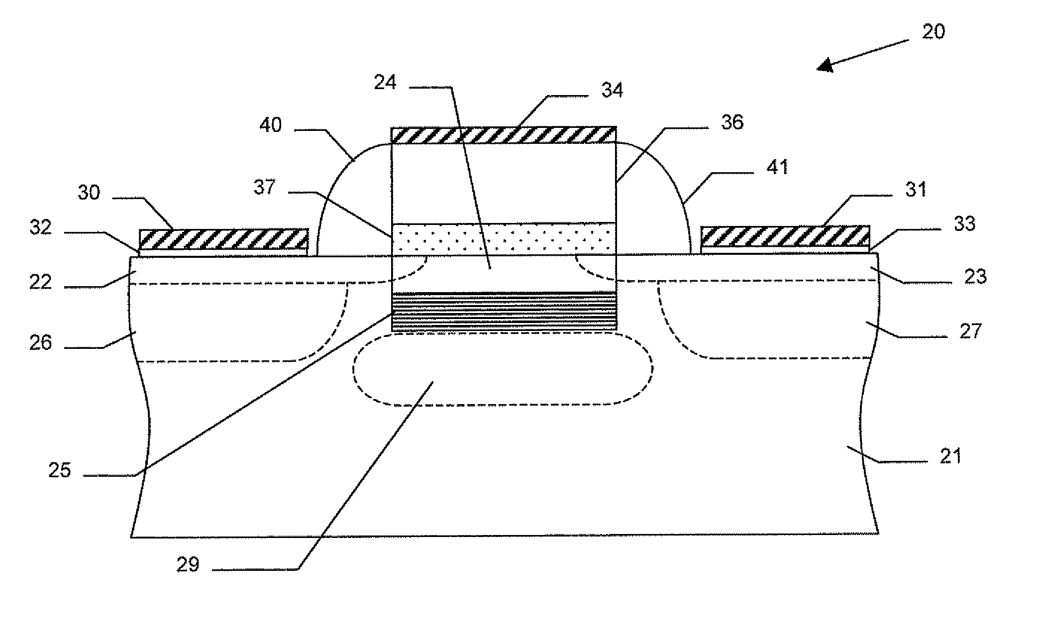
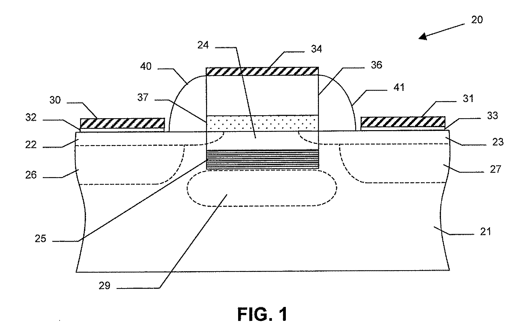
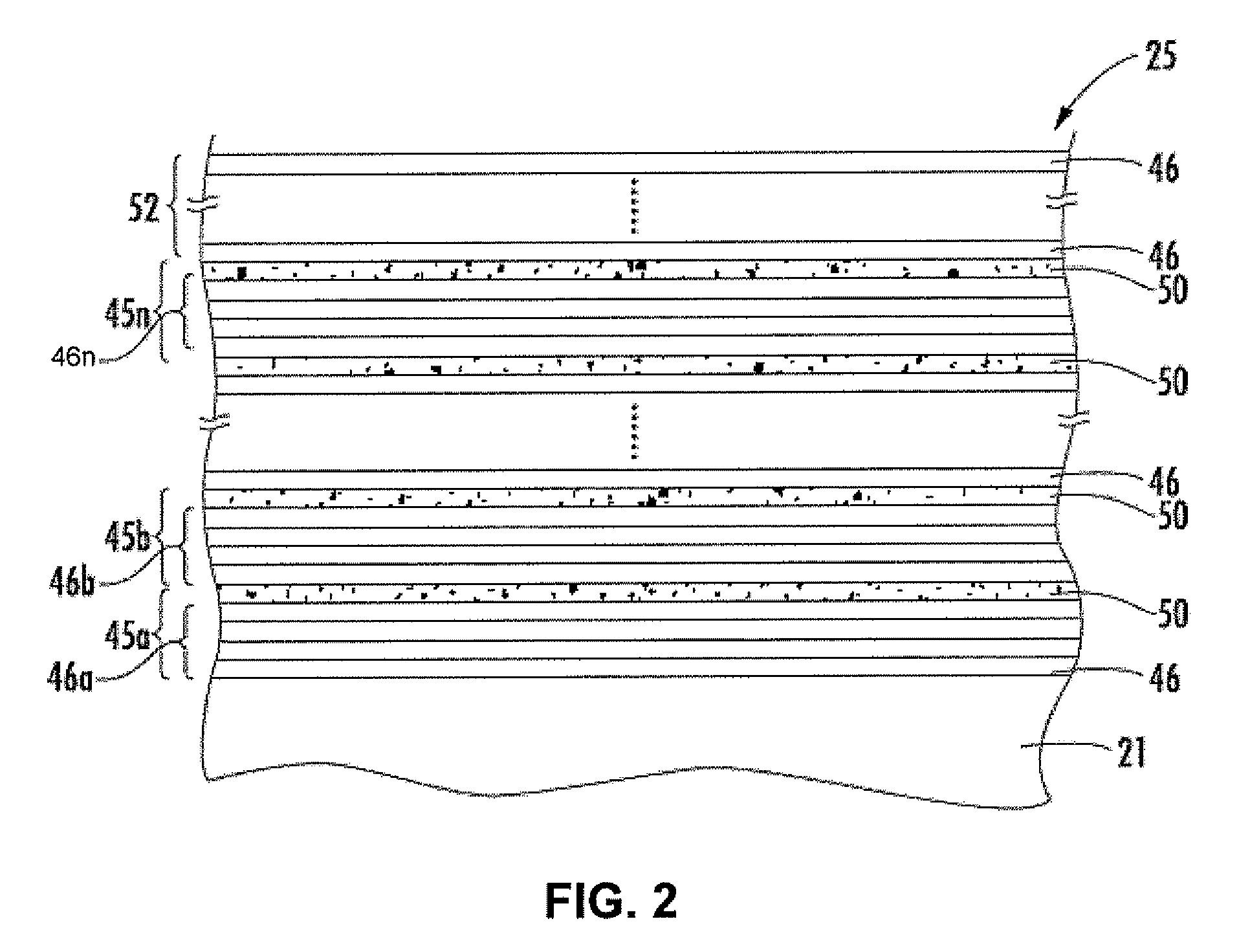
[0027] The present invention will now be described more fully hereinafter with reference to the accompanying drawings, in which preferred embodiments of the invention are shown. This invention may, however, be embodied in many different forms and should not be construed as limited to the embodiments set forth herein. Rather, these embodiments are provided so that this disclosure will be thorough and complete, and will fully convey the scope of the invention to those skilled in the art. Like numbers refer to like elements throughout, and prime notation is used to indicate similar elements in alternate embodiments.

[0028] The present invention relates to controlling the properties of semiconductor materials at the atomic or molecular level to achieve improved performance within semiconductor devices. Further, the invention relates to the identification, creation, and use of improved materials for use in the conduction paths of semiconductor devices.

[0029] Applicants theorize, without...


PUM


Abstract

A method for making a semiconductor device may include forming at least one metal oxide field-effect transistor (MOSFET) by forming a body, forming a dopant blocking superlattice adjacent the body, and forming a channel layer adjacent the dopant blocking superlattice and opposite the body. The dopant blocking superlattice may include a plurality of stacked groups of layers. Each group of layers of the dopant blocking superlattice may include a plurality of stacked base semiconductor monolayers defining a base semiconductor portion and at least one non-semiconductor monolayer constrained within a crystal lattice of adjacent base semiconductor portions.

Description

CROSS-REFERENCE TO RELATED APPLICATIONS [0001] This application is a continuation-in-part of U.S. patent application Ser. No. 10 / 992,422 filed Nov. 18, 2004, which is a continuation of U.S. patent application Ser. No. 10 / 647,060 filed Aug. 22, 2003, which is a continuation-in-part of U.S. patent application Ser. Nos. 10 / 603,696 and 10 / 603,621 filed on Jun. 26, 2003, the entire disclosures of which are incorporated by reference herein.FIELD OF THE INVENTION [0002] The present invention relates to the field of semiconductors, and, more particularly, to semiconductors having enhanced properties such as based upon energy band engineering and associated methods. BACKGROUND OF THE INVENTION [0003] Structures and techniques have been proposed to enhance the performance of semiconductor devices, such as by enhancing the mobility of the charge carriers. For example, U.S. Patent Application No. 2003 / 0057416 to Currie et al. discloses strained material layers of silicon, silicon-germanium, and...

Claims


Application Information

Patent Timeline
IPC IPC(8): H01L29/06
CPCB82Y10/00H01L21/823807H01L29/1054H01L29/7833H01L29/151H01L29/152H01L29/155H01L29/1083
Inventor STEPHENSON, ROBERT JOHNHYTHA, MAREK
Owner MEARS TECH
Why Eureka
Try Eureka