Evaluation semiconductor device

a semiconductor and device technology, applied in the field of semiconductor devices, can solve the problems of disadvantageous late practice of countermeasures, inability to employ the method of patent literature 1 for evaluating detection, and time-consuming teg formation

Inactive Publication Date: 2006-12-07
PANASONIC CORP
View PDF8 Cites 7 Cited by
  • Summary
  • Abstract
  • Description
  • Claims
  • Application Information

AI Technical Summary

Benefits of technology

[0024] Furthermore, the performance of a current measurement apparatus is recently improved and hence the accuracy and the speed for measuring a current are largely improved. Therefore, when a large number of small-scaled patterns are included in each test group element of the invention, a soft open or a soft short, which is conventionally impossible to detect, can be detected and evaluated.
[0026] Also, when the yield of each layer is evaluated by using the evaluation semiconductor device of the invention, the respective processes for the fabrication of a DRAM can be developed in parallel, and hence, TAT (turn-around-time) of the process development can be shortened.
[0027] Furthermore, when the relationship between the yield obtained by using the evaluation semiconductor device of the invention and the yield of each failure item of an actual product is previously found, the yield of each process can be calculated on the basis of the yield of the failure item in the fabrication of the actual product. Specifically, even when there arises a problem of lowering of the yield or the like in the mass-production of the actual product, a process possibly causing the problem can be found on the basis of the yield of each failure item, and hence, the problem can be coped with at an early stage.

Problems solved by technology

However, in the case where the TEG for the DRAM portion having the same layout as that of an actual product is repeatedly formed as in the aforementioned conventional method, the formation of the TEG takes time.
Therefore, when a problem actually arises in a process, it takes time to detect the problem, and hence, practice of a countermeasure is disadvantageously late.
However, it is impossible to employ the method of Patent Literature 1 for evaluating detection results dividedly in respective processes in forming the capacitor cell.

Method used


Image

  • Evaluation semiconductor device
  • Evaluation semiconductor device
  • Evaluation semiconductor device

Examples


Embodiment Construction

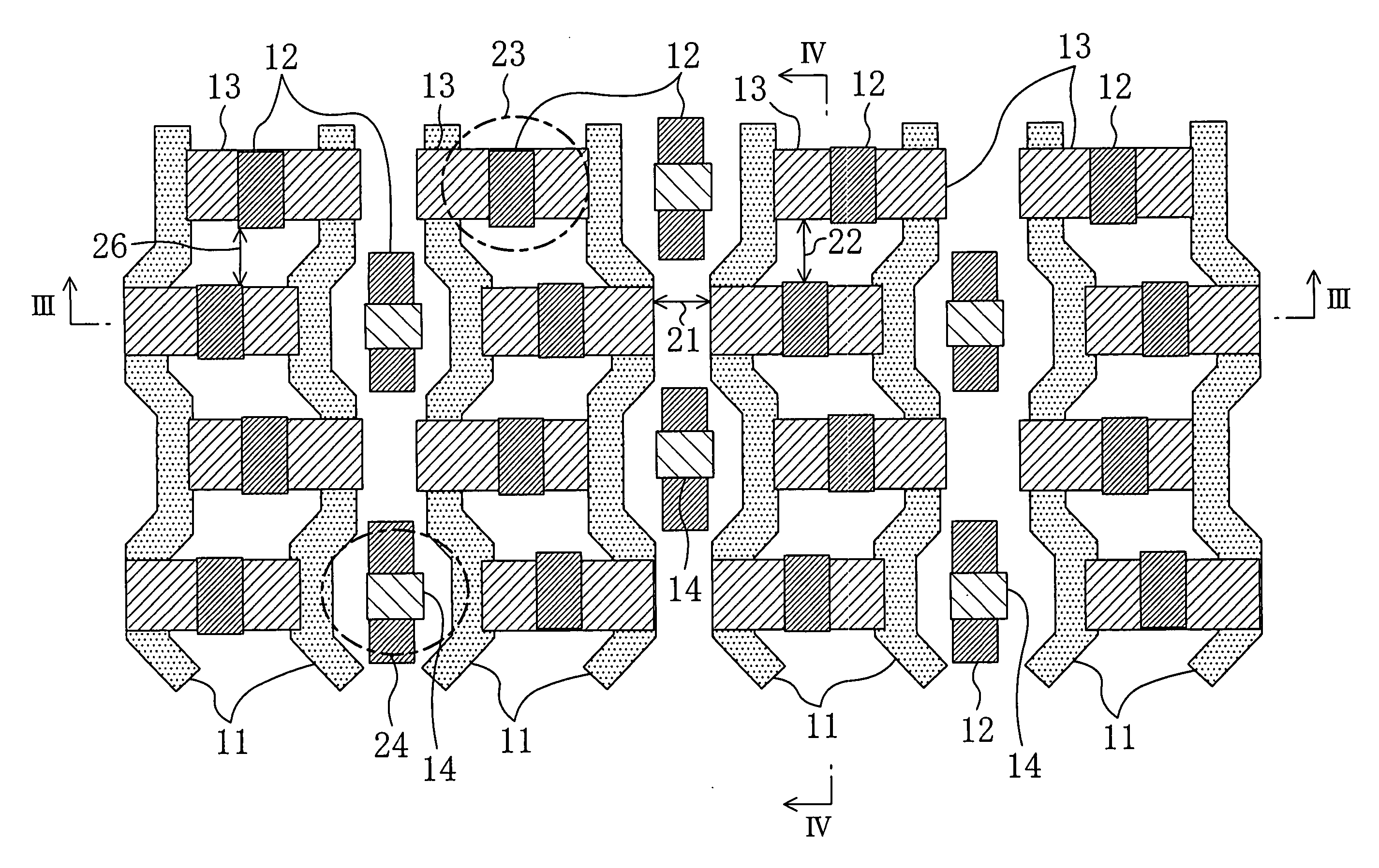
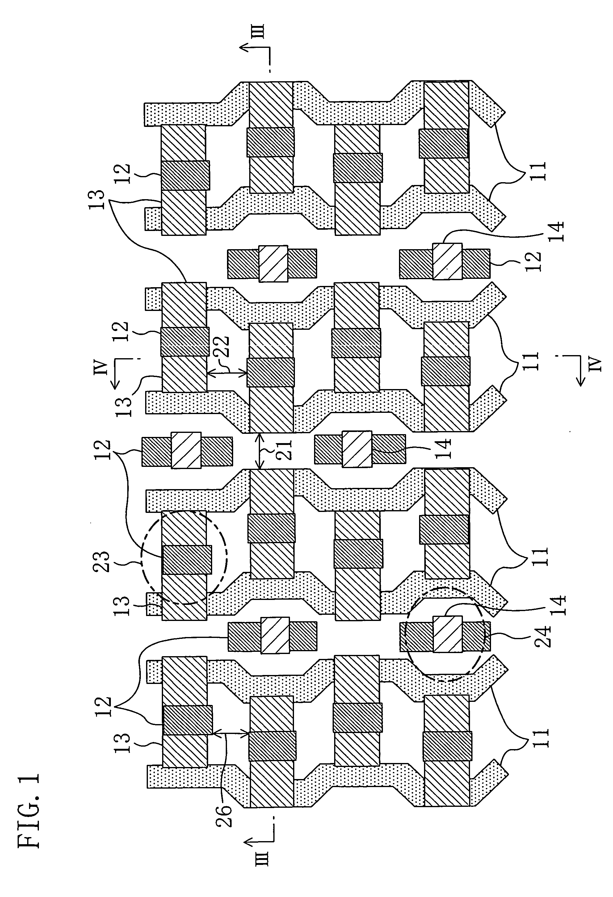
[0046] A DRAM yield calculation TEG and a yield calculation method using the same according to an embodiment of the invention will now be described with reference to the accompanying drawings. Each DRAM yield calculation TEG of this embodiment described below is formed by providing a necessary interconnect to a mask layer disposed on or beneath a target mask layer to be calculated for the yield, so that the yield of a DRAM portion of an integrated circuit device can be obtained as a product of yields (fraction defectives) attained in processes respectively corresponding to principal mask layers.

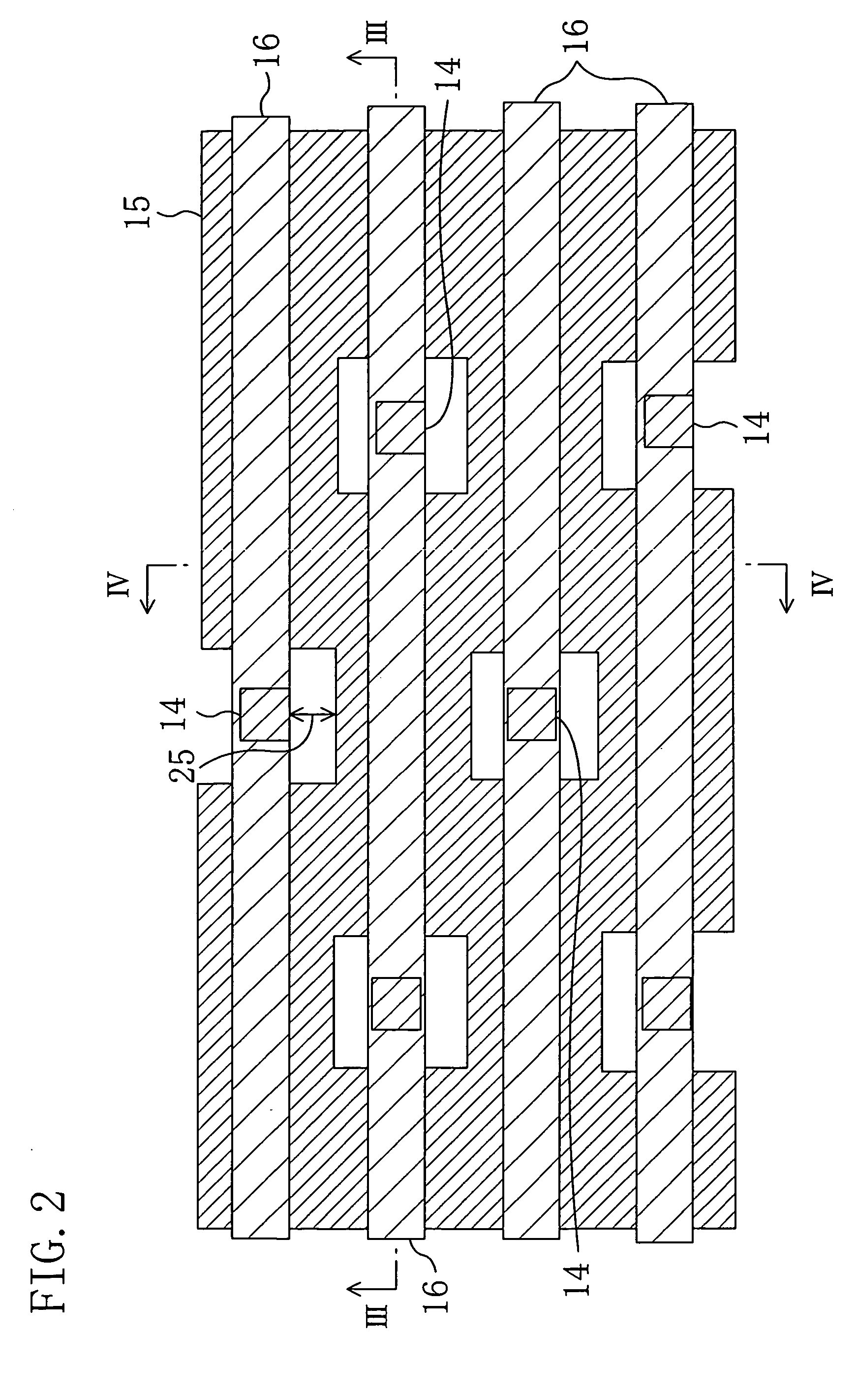
[0047]FIGS. 1 and 2 show the plane structure of the DRAM portion of the integrated circuit device to be evaluated for the yield, and specifically, FIG. 1 is a plan view of a layer where a storage plate of a capacitor is provided and a layer disposed beneath this layer, and FIG. 2 is a plan view of a layer where an upper cell plate of the capacitor is provided and a layer disposed on this lay...


PUM


Abstract

An evaluation semiconductor device is used for evaluating a yield of a DRAM portion of an integrated circuit device. The evaluation semiconductor device includes an evaluation gate interconnect provided in a layer corresponding to a gate interconnect layer of the DRAM portion; and an evaluation source contact corresponding to a source contact of a capacitor included in the DRAM portion and connected to the evaluation gate interconnect.

Description

BACKGROUND OF THE INVENTION [0001] The present invention relates to an evaluation semiconductor device (TEG: test element group) provided with appropriate interconnects for obtaining a yield of a semiconductor integrated circuit device including a capacitor cell as a product of process yields attained in respective principal mask layer. [0002] In fabrication of semiconductor devices such as LSIs, the cost for the semiconductor devices can be lowered by obtaining a large number of good LSIs from one semiconductor substrate (semiconductor wafer), namely, by improving the yield. On the other hand, one of known causes to lower the yield is, for example, a defect such as a foreign matter caused in each process (wiring process in particular) of the LSI fabrication process, which leads to a short or an open or a formation failure of a capacitor. The density of defects such as a foreign matter can be estimated on the basis of, for example, dust distribution information of a clean room where...

Claims


Application Information

Patent Timeline
Patent Type & Authority Applications(United States)
IPC IPC(8): H01L27/108
CPCH01L27/0207H01L27/10882H01L27/10811H10B12/312H10B12/48
Inventor TOHYAMA, YOKOOKUNO, YASUTOSHI
Owner PANASONIC CORP
Why Eureka
Try Eureka