Radiation curable conductive ink and manufacturing method for using the same

a technology of conductive ink and manufacturing method, which is applied in the direction of non-metal conductors, conductors, organic conductors, etc., can solve the problems of current technology being unable to overcome the problem, many innovative products or new business modes are still speculative and non-viable, and the current manufacturing cost is still very high. , to achieve the effect of reducing cost, rapid curable, and shortening working procedur

Inactive Publication Date: 2006-12-14
YANG YUNG SHU
View PDF3 Cites 23 Cited by
  • Summary
  • Abstract
  • Description
  • Claims
  • Application Information

AI Technical Summary

Benefits of technology

[0031] A manufacturing method for conductive substrate using screen printing is realized using the aforementioned components of the radiation curable conductive ink of the present invention, thereby foreshortening working procedure and reducing cost, wherein method adopted is disclosed below:
[0056] A manufacturing method for conductive substrate using screen printing is realized using the aforementioned radiation curable conductive ink of the present invention and the method of using conductive ink to manufacture the conductive substrate, thereby achieving objectives of foreshortening working procedure and reducing cost. The method is particularly applicable for applications in radio frequency identification RFID antenna, printed-circuit boards, smart cards (non-contact chip cards) component members, smart labels, printed electronics, anti-EMI and anti-static materials.
[0057] Furthermore, the radiation curable conductive ink mixed with the aforementioned components undergoes a chemical crooslinking reaction that generally occurs within a few seconds compared to between 3 minutes to 2 hours and a temperature around 80° C.-220° C. needed by general thermal curable resins (for example: thermal curable type epoxy resin and polyester resin), thereby providing the present invention with advantages of rapid curable and energy savings.
[0058] After the conductive powder applied by combining properties of the aforementioned materials has undergone radiation crosslinking, apart from having the advantage of rapid curing speed, moreover, the resulting conductive substrate is provided with superior electrical conductivity and resistance to oxidation.
[0059] In addition, because of a light-screening effect and high specific gravity of the conductive powder, rapid sedimentation of the metallic powder easily causes, which makes it difficult for the radiation curable conductive ink to achieve an ideal degree of cure. Moreover, it is difficult for the metallic powder to be uniformly dispersed and achieve a substantially thick conductive ink.
[0060] The present invention has made improvements that resolve the aforementioned shortcomings, and enables the radiation curable conductive ink to undergo a rapid and curing reaction that achieves favorable metallic powder dispersibility and superior electrical conductivity, as well as superior electrical conductivity stability, resistance to oxidation and low cost.

Problems solved by technology

Although lamination of the aforementioned laminate type antenna, printed-circuit boards and radio frequency identification systems offer convenience of use, however, the current cost of manufacture is still very high, with the result that many innovative products or new modes of business are still speculative and non-viable.
However, current technology is still unable to overcome the problem of the high cost of radio frequency identification systems, primarily because of the high cost of the aforementioned antenna compared, which can cost higher than the chips.
However, even mass production is unable to reduce costs because of complications in the job program.
Even though current technology has enabled the universal adoption of screen printing in the manufacture of circuit substrate, however, the current primary use of traditional thermal curable conductive ink containing pure silver powder is unable to effectively reduce manufacturing costs when used on the aforementioned radio frequency identification antenna or circuit board.

Method used


Image

  • Radiation curable conductive ink and manufacturing method for using the same
  • Radiation curable conductive ink and manufacturing method for using the same
  • Radiation curable conductive ink and manufacturing method for using the same

Examples


Embodiment Construction

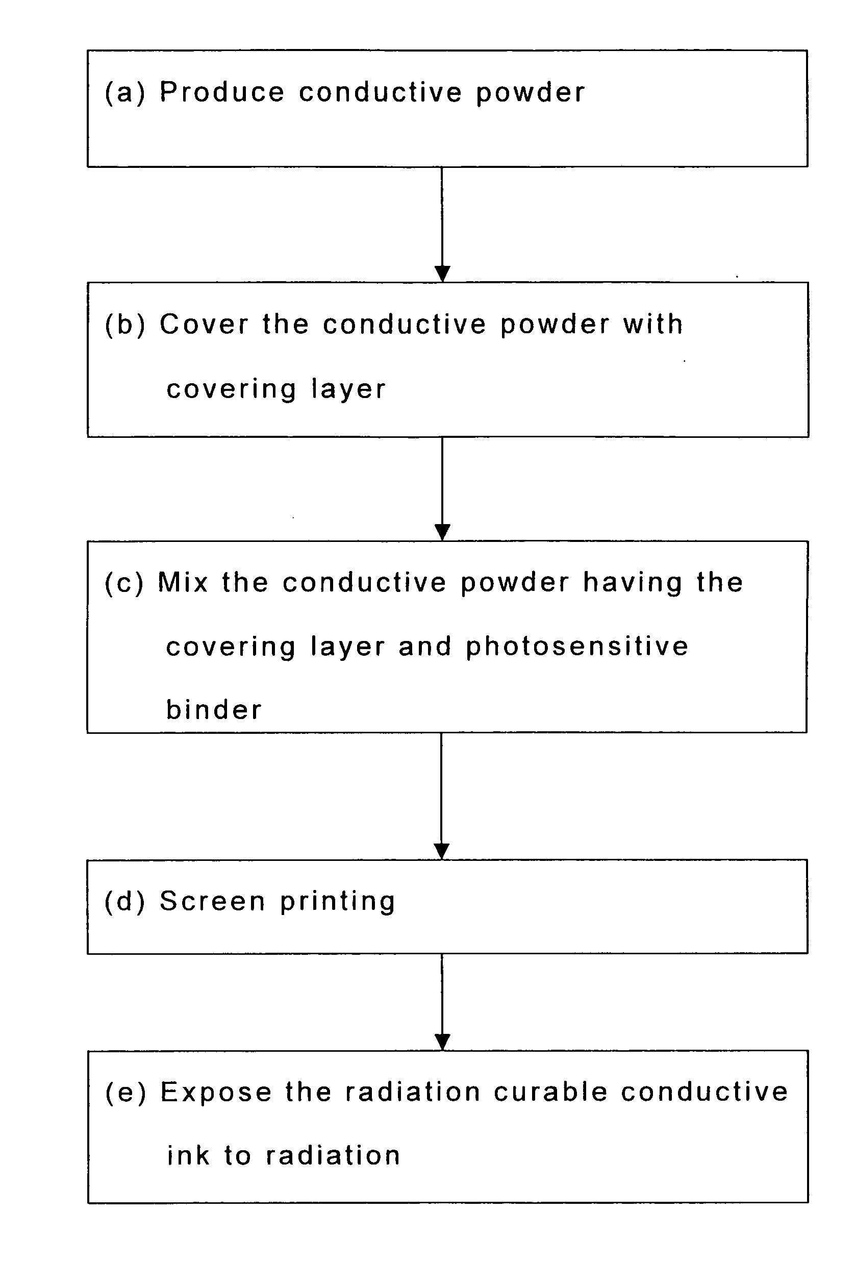
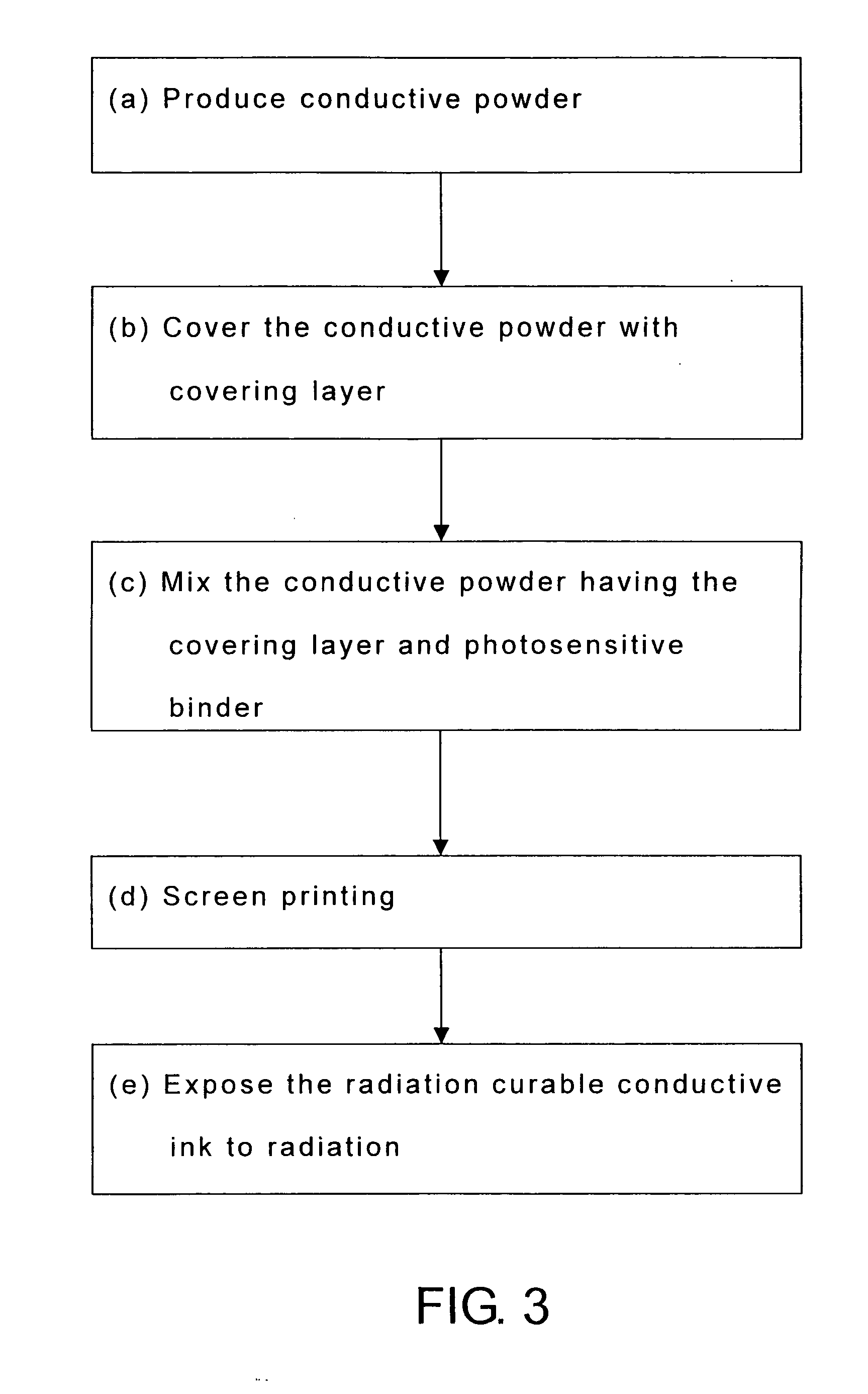
[0066] A radiation curable conductive ink of the present invention undergoes a chemical crosslinking reaction by irradiating conductive ink with radiation, wherein the conductive ink contains at least the following components: [0067] (a) Conductive powder having a covering layer, wherein the weight of the silver content of the conductive powder before covering with the covering layer having less than 90% by weight of silver content, more than 30% by weight of copper or more than 30% by weight of aluminum; [0068] (b) The covering layer covering surface of the conductive powder, wherein weight of silver content of the covering layer accounts for more than 30% of the weight of the covering layer, and the weight of the covering layer accounts for less than 80% of the total weight of the conductive powder and the covering layer; [0069] (c) The conductive powder having the covering layer, wherein average size of conductive powder is less than 40 micro; [0070] (d) A photosensitive binder h...


PUM

PropertyMeasurementUnit
temperatureaaaaaaaaaa
wavelength rangeaaaaaaaaaa
wavelengthaaaaaaaaaa

Abstract

The present invention provides a radiation curable conductive ink and a manufacturing method for conductive substrate using the conductive ink, wherein components of the radiation curable conductive ink contain at least conductive powder having a covering layer and a photosensitive binder. The radiation curable conductive ink is printed on surface of a substrate using a screen printing method, and a chemical crosslinking reaction is achieved by irradiating the conductive ink with ultraviolet ray, visible light or electron beam, thereby forming a conductive substrate. The conductive substrate is particularly applicable for use in laminate type electronic devices, including radio frequency identification (RFID) antenna, printed-circuit boards, smart cards (non-contact chip cards) components, smart labels, printed electronics, anti-electromagnetic interference (EMI) and anti-electrostatic materials.

Description

BACKGROUND OF THE INVENTION [0001] (a) Field of the Invention [0002] The present invention relates to a radiation curable conductive ink and manufacturing method for conductive substrate using conductive ink, which is particularly applicable for use in electronic materials, including radio frequency identification (RFID) antenna, printed-circuit boards, smart cards (non-contact chip cards) components, smart labels, printed electronics, anti-electromagnetic interference (EMI) and anti-electrostatic materials. [0003] (b) Description of the Prior Art [0004] The driving force of technological progress has accentuated multifunctionality and continuous miniaturization in the design of various electronic products. More particularly, rapid development in networking and wireless communication in recent years has seen the perpetual modification in a diverse range of portable electronic products, which has altered the unlimited potentiality of 21st century modes of business. [0005] There is an...

Claims


Application Information

Patent Timeline
Patent Type & Authority Applications(United States)
IPC IPC(8): C08F2/46B05D1/12B05D5/00H01B1/12
CPCB05D1/32B05D3/067B05D5/12B41M1/12B41M7/0081C09D11/52H05K1/095H05K2201/0218C09D11/101
Inventor YANG, YUNG-SHU
Owner YANG YUNG SHU
Why Eureka
Try Eureka