Substrate-free flip chip light emitting diode and manufacturing method thereof

a technology of light-emitting diodes and flip-chips, which is applied in the direction of basic electric elements, semiconductor devices, electrical equipment, etc., can solve the problems of reducing the life reducing the cost of the substrate having a better light-emitting capacity such as sapphire, and reducing the cost of the conventional led device. , to achieve the effect of reducing the cost of the led device, enhancing heat-sink efficiency, and simplify

Inactive Publication Date: 2006-12-14
CHUNGHWA PICTURE TUBES LTD
View PDF6 Cites 19 Cited by
  • Summary
  • Abstract
  • Description
  • Claims
  • Application Information

AI Technical Summary

Benefits of technology

[0010] Accordingly, the present invention is directed to a substrate-free LED device and manufacturing method thereof, wherein the LED device does not need a conventional transparent substrate. Therefore, the cost of the LED device is reduced, the heat-sink efficiency is enhanced and the manufacturing process of the LED device is simplified.
[0040] Accordingly, in the LED device of the present invention, since the substrate of the conventional LED is replaced by the high heat-sink substrate disposed in the other side of the epitaxial layer, the heat-sink efficiency is enhanced and the structure strength of the LED device is maintained. In addition, since the high heat-sink, high transparent protection layer is provided, the light transmittance of the surface of the LED device is excellent, and thus the light emitting efficiency of the LED device is also excellent. Moreover, the surface of the LED device of the invention does not need to be polished. Accordingly, the present invention provides a high light emitting efficiency, high heat-sink efficiency, low-cost, simple process, and high yield LED device and manufacturing method thereof.

Problems solved by technology

Thus, the life period of the conventional LED device is reduced.
In addition, the substrate having a better light transmittance such as sapphire is very expensive, if a substance having poor light transmittance is provided, the cost may be reduced but the light emitting efficiency of the conventional LED device is also reduced.
Moreover, to enhance the light transmittance of the conventional LED device, the surface of the transparent substrate 124 has to be polished, thus the process is more complex and the yield of the process is reduced.

Method used


Image

  • Substrate-free flip chip light emitting diode and manufacturing method thereof
  • Substrate-free flip chip light emitting diode and manufacturing method thereof
  • Substrate-free flip chip light emitting diode and manufacturing method thereof

Examples


Embodiment Construction

[0046] The present invention now will be described more fully hereinafter with reference to the accompanying drawings, in which preferred embodiments of the invention are shown. This invention may, however, be embodied in many different forms and should not be construed as limited to the embodiments set forth herein; rather, these embodiments are provided so that this disclosure will be thorough and complete, and will fully convey the scope of the invention to those skilled in the art. Like numbers refer to like elements throughout.

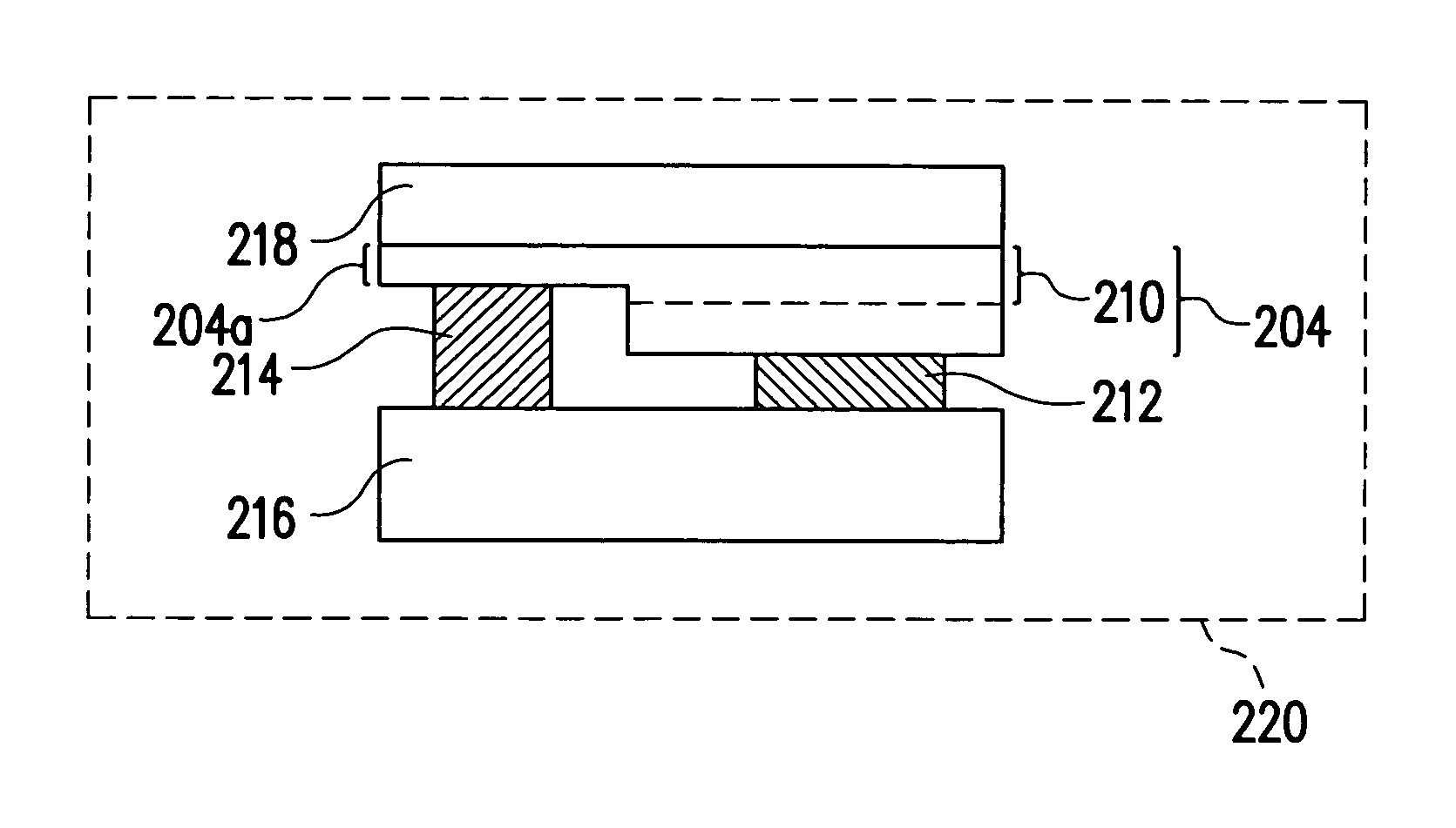
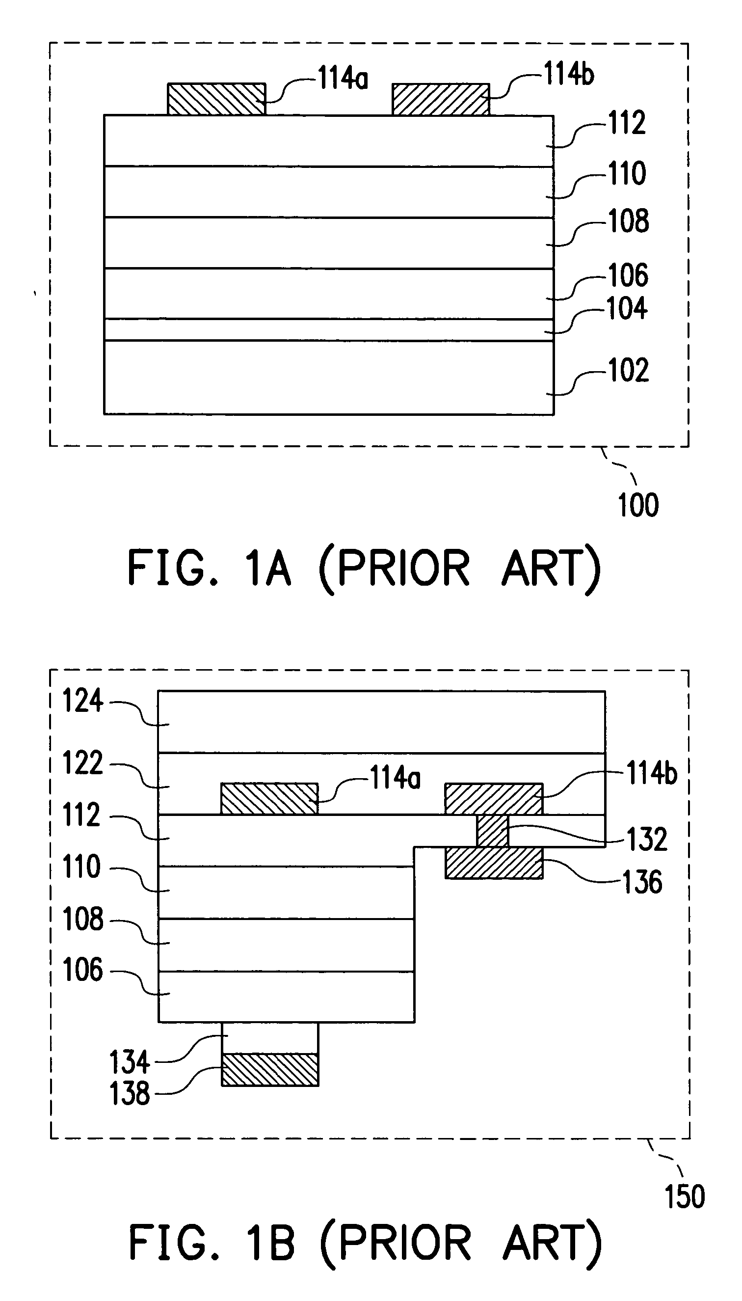
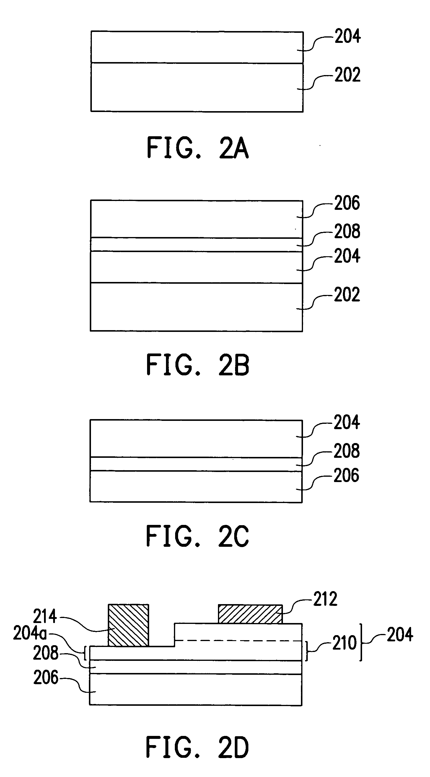
[0047]FIG. 2A to FIG. 2G are cross-sectional views schematically illustrating a process flow for manufacturing a LED device according to one embodiment of the present invention. Referring to FIG. 2A, first of all, a first substrate 202 is provided. In one embodiment of the invention, the first substrate 202 comprises, for example but not limited to, gallium arsenide (GaAs), aluminum oxide (Al2O3) or silicon carbide (SiC) substrate. In addition, the first...


PUM


Abstract

A substrate-free LED device is provided. The LED device comprises a substrate, an epitaxial layer disposed on the substrate, a first electrode disposed on a portion of the epitaxial layer, a second electrode disposed on another portion of the epitaxial layer, and a protection layer, disposed over the epitaxial layer. It is noted that in the LED device, the substrate comprises, for example but not limited to, high heat-sink substrate, and the protection layer comprises, for example but not limited to, high heat-sink, high transparent material.

Description

BACKGROUND OF THE INVENTION [0001] 1. Field of the Invention [0002] The present invention generally relates to a light emitting diode and manufacturing method thereof. More particularly, the present invention relates to a substrate-free flip chip light emitting diode and manufacturing method thereof. [0003] 2. Description of Related Art [0004] Light emitting diode (LED) is a semiconductor component that has been broadly used as light emission device. The light emitting chip of the LED is generally comprised of III-V compound semiconductor such as gallium phosphide (GaP), gallium arsenide (GaAs), or gallium nitride (GaN). The principle of light emission of LED is the transformation of electrical energy into light energy, which is performed by applying current to the compound semiconductor to generate electrons and holes. Thereafter, an excess energy is released by the combination of electrons and holes, and thus the LED emits light. In general, the LED has the advantages of fast resp...

Claims


Application Information

Patent Timeline
Patent Type & Authority Applications(United States)
IPC IPC(8): H01L29/22
CPCH01L21/6835H01L33/0079H01L2221/6835H01L2221/68368H01L2924/12041H01L2224/73253H01L2924/01079H01L24/27H01L2224/274H01L2224/06102H01L33/0093
Inventor CHEN, CHING-CHUNG
Owner CHUNGHWA PICTURE TUBES LTD
Why Eureka
Try Eureka