Phase change memory device having an adhesion layer and manufacturing process thereof

a memory device and adhesion layer technology, applied in the direction of semiconductor devices, basic electric elements, electrical apparatus, etc., can solve the problems of destroying the phase change capability and difficult to integrate gst alloys into semiconductor processing, and achieve effective reduction of titanium diffusion, good adhesion, and less diffusion

Inactive Publication Date: 2006-12-14
STMICROELECTRONICS SRL
View PDF7 Cites 53 Cited by
  • Summary
  • Abstract
  • Description
  • Claims
  • Application Information

AI Technical Summary

Benefits of technology

[0007] In one embodiment, the present invention provides a glue material with good adhesion and less diffusion in GST alloys than present materials. In particular, an adhesion layer is described herein, which is in contact with a phase change memory material layer, the adhesion layer including titanium and a component, such as silicon, in a quantity sufficient to effectively reduce the diffusion of titanium without substantially affecting the adhesion properties of the adhesion layer.

Problems solved by technology

In fact, it is very difficult to integrate GST alloys into semiconductor processing since they do not adhere to most of the stable dielectrics.
Some metallic materials (e.g., Ti) show good adhesion with GST alloys, but they tend to diffuse into GST alloys, react with the constituent elements, and kill the phase change capability.

Method used


Image

  • Phase change memory device having an adhesion layer and manufacturing process thereof
  • Phase change memory device having an adhesion layer and manufacturing process thereof
  • Phase change memory device having an adhesion layer and manufacturing process thereof

Examples


Embodiment Construction

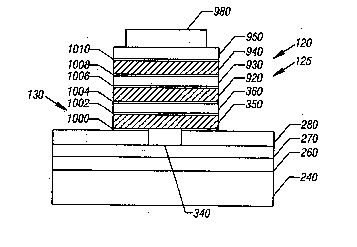
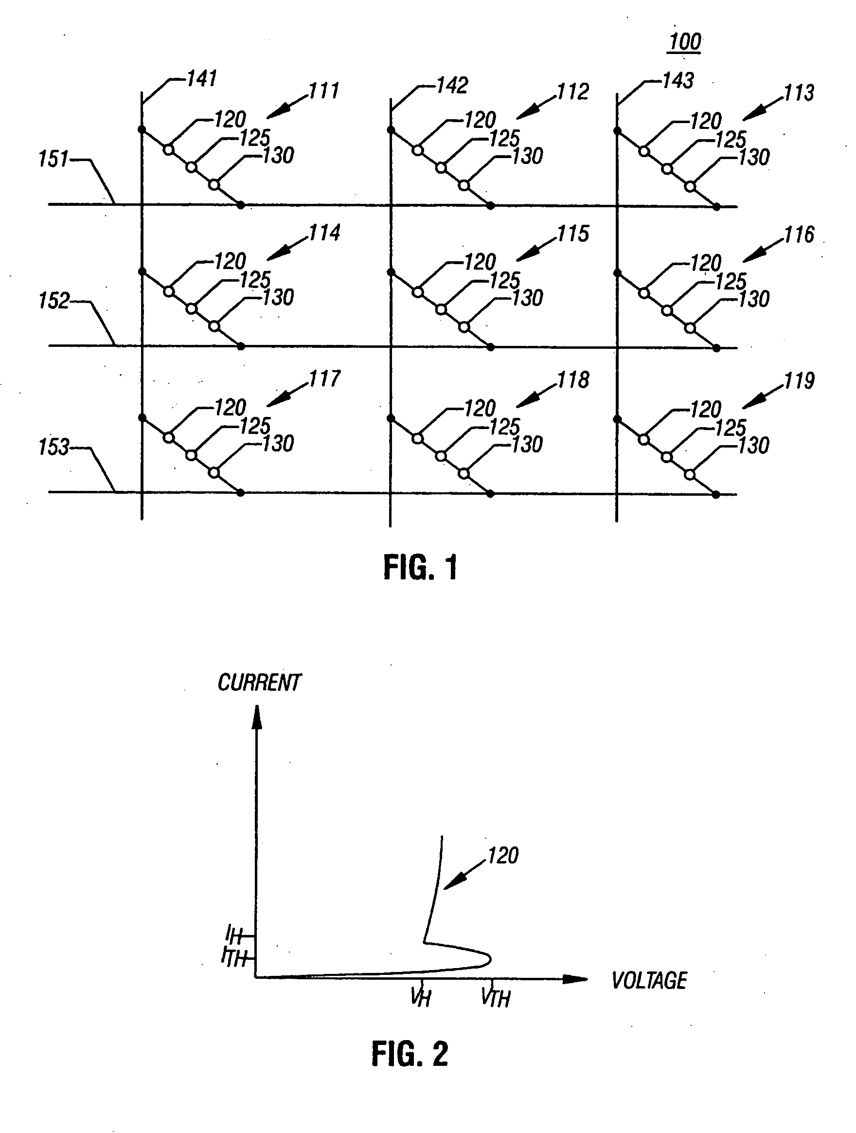
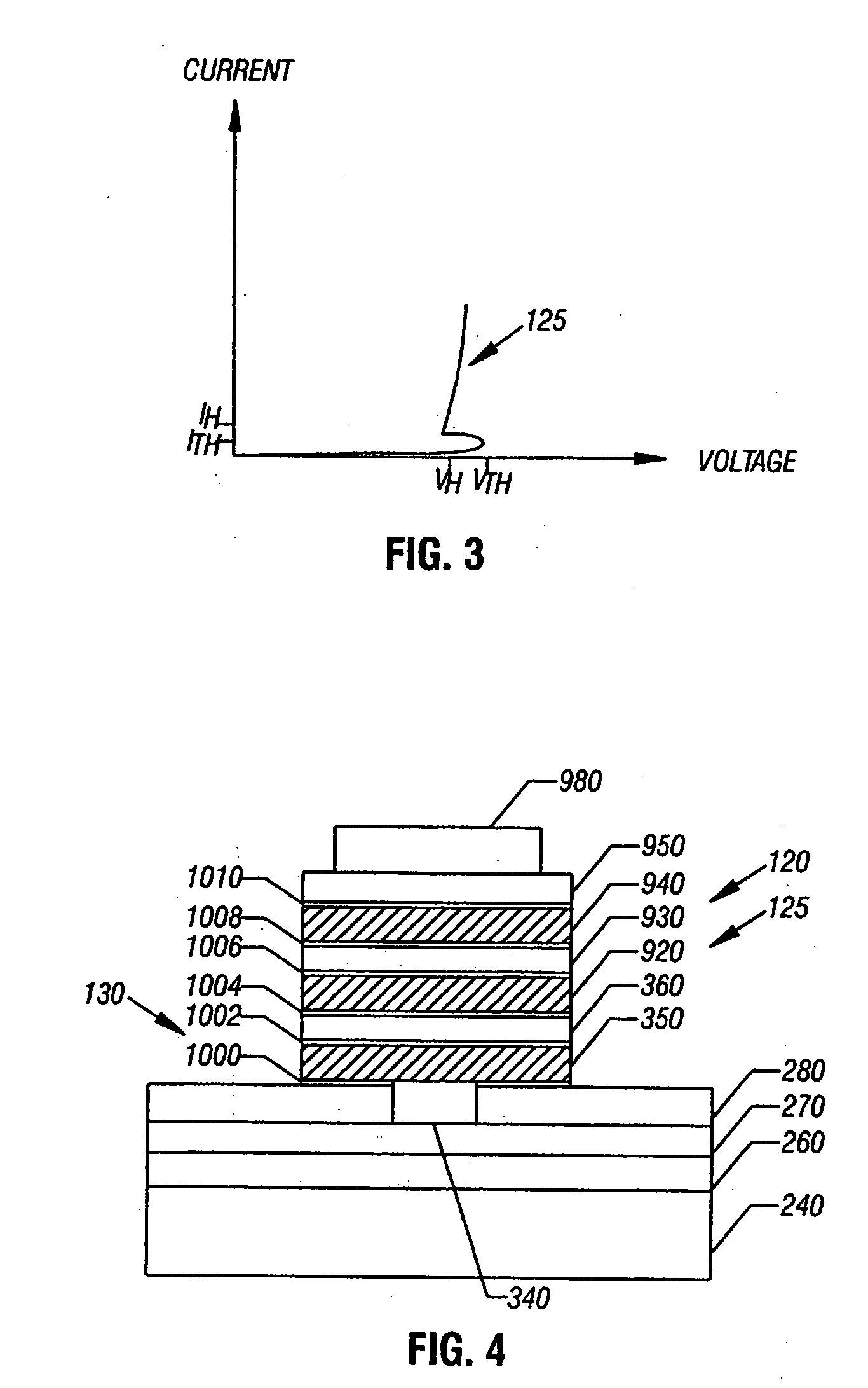
[0016]FIG. 1 shows an embodiment of a memory 100. Memory 100 includes an n×n array of memory cells 111-119, each including a first select device 120, a second select device 125, and a memory element 130.

[0017] Memory elements 130 comprises a phase change material and thus may be referred to as a phase change memory. A phase change material is a material having electrical properties (e.g., resistance, capacitance, etc.) that may be changed through the application of energy such as, for example, heat, light, voltage potential, or electrical current. Examples of a phase change material include a chalcogenide material.

[0018] Memory 100 includes column lines 141-143 and row lines 151-153 to select a particular memory cell of the array during a write or read operation. Column lines 141-143 and row lines 151-153 may also be referred to as word lines or address lines since these lines are used to address memory cells 111 -119 during programming or reading. Column lines 141-143 may also be...


PUM

PropertyMeasurementUnit
thickaaaaaaaaaa
thicknessaaaaaaaaaa
resistanceaaaaaaaaaa

Abstract

A memory includes a phase change memory element having a memory layer of a calcogenide material and a glue layer of an alloy of the form TiaXbNc where X is selected in the group comprising silicon, aluminum, carbon, or boron, and c may be 0. The nitrogen and silicon are adapted to reduce the diffusion of titanium toward the chalcogenide layer.

Description

BACKGROUND OF THE INVENTION [0001] 1. Field of the Invention [0002] This invention relates generally to a phase change memory device having an adhesion layer and to the manufacturing process thereof. [0003] 2. Description of the Related Art [0004] Phase change memory devices use phase change materials, i.e., materials that may be electrically switched between a generally amorphous and a generally crystalline state, for electronic memory application. One type of memory element utilizes a phase change material that is electrically switched between a structural state of generally amorphous and generally crystalline local order or between different detectable states of local order across the entire spectrum between completely amorphous and completely crystalline states. The state of the phase change materials is also non-volatile in that, when set in either a crystalline, semi-crystalline, amorphous, or semi-amorphous state representing a resistance value, that value is retained until c...

Claims


Application Information

Patent Timeline
Patent Type & Authority Applications(United States)
IPC IPC(8): H01L29/768
CPCH01L45/04H01L45/06H01L45/12H01L45/1233H01L27/2427H01L45/141H01L45/144H01L45/16H01L45/126H10B63/24H10N70/801H10N70/20H10N70/8413H10N70/882H10N70/231H10N70/011H10N70/8828H10N70/826
Inventor CHANG, KUO-WEILEE, JONG-WON S.BESANA, PAOLA
Owner STMICROELECTRONICS SRL
Why Eureka
Try Eureka