Electric signal splitters

a technology of electric signals and splitters, applied in the direction of waveguides, waveguide type devices, coupling device connections, etc., can solve the problems of valuable space consumption by mounting types, and achieve the effects of consuming valuable space, and reducing the size of the splitter casing

Inactive Publication Date: 2006-12-14
GALE ROBERT D
View PDF59 Cites 12 Cited by
  • Summary
  • Abstract
  • Description
  • Claims
  • Application Information

AI Technical Summary

Benefits of technology

[0016] Additionally, the present invention, by the unique design, has reduced the size of the splitter casing and allows the use of a multi-port splitter in smaller areas, such as a standard electrical outlet box with additional connections in the same outlet box such as a telephone jack or modem jack. This reduced size is accomplished by the incorporation of component recesses or voids constructed into the printed circuit board (PCB) of the splitter. The PCB uses the most current technology in the art of splitters. The PCB contains transformers or splitter cores for each output port on the splitter as well as other electrical components common in the art of electronic signal splitters. Splitter cores generally are soldered to the surface of the PCB of conventional type splitters, and this type of mounting consumes valuable space. The present invention contains component voids and thus optimizes the use of space within a splitter box and overcomes the problem by disposing the splitter cores within the component voids.
[0017] Further, the present invention presents through the unique size of the case and construction of the PCB provides an advantage over conventional devices by reducing signal insertion loss. For applications that utilize reverse path the present invention also reduces return loss.
[0018] Additionally, more and more h

Problems solved by technology

Splitter cores generally are soldered to the surface of the PCB of conven

Method used


Image

  • Electric signal splitters
  • Electric signal splitters
  • Electric signal splitters

Examples


Embodiment Construction

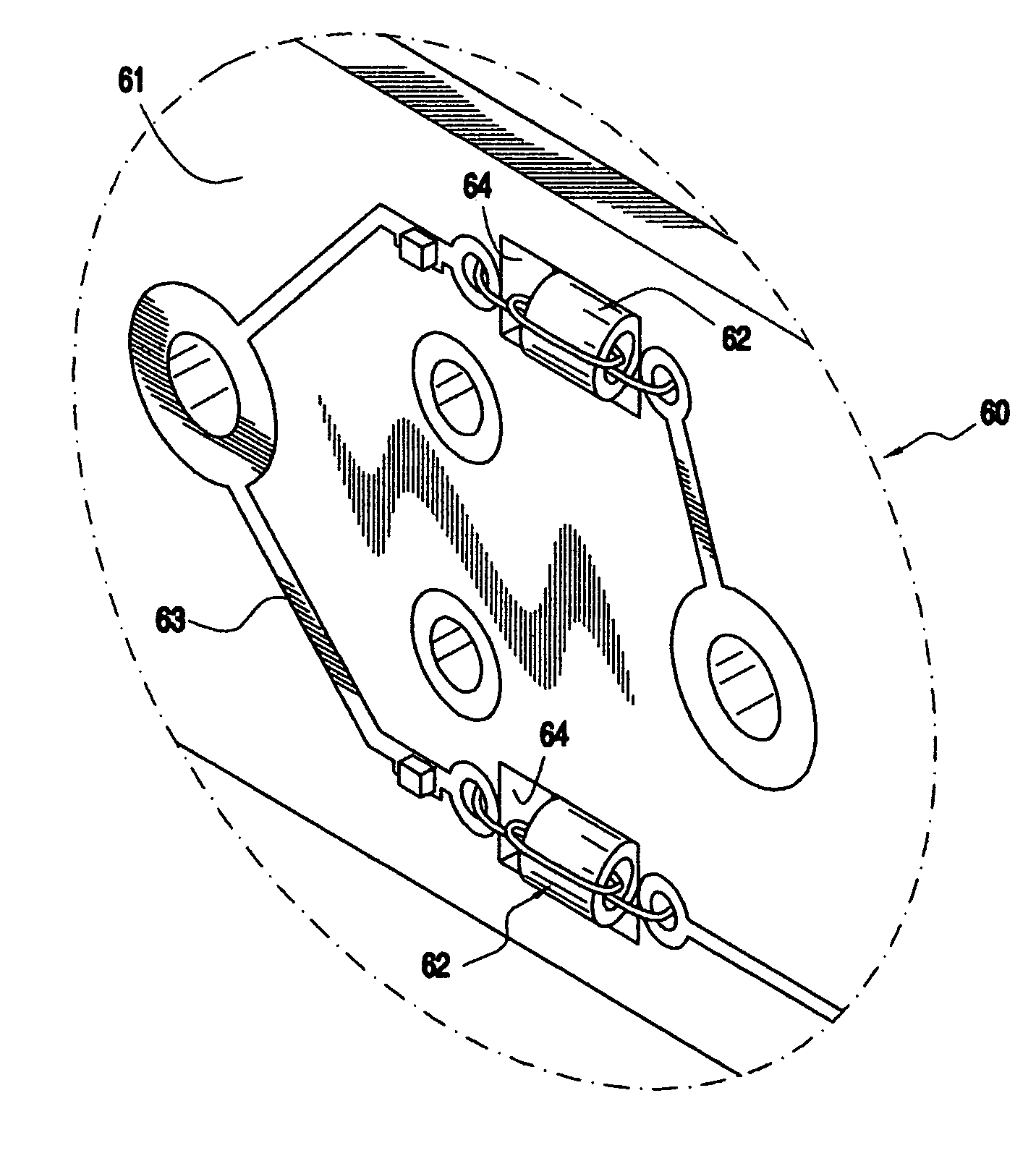
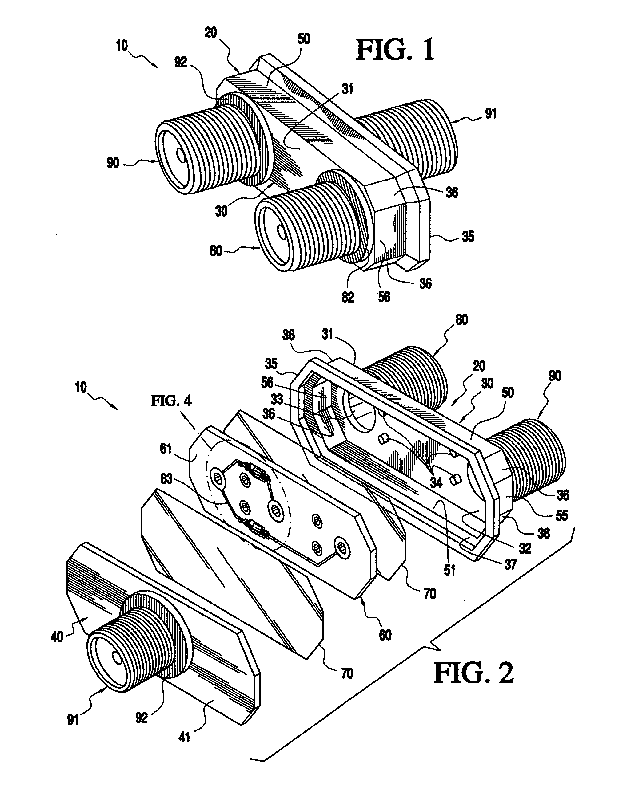
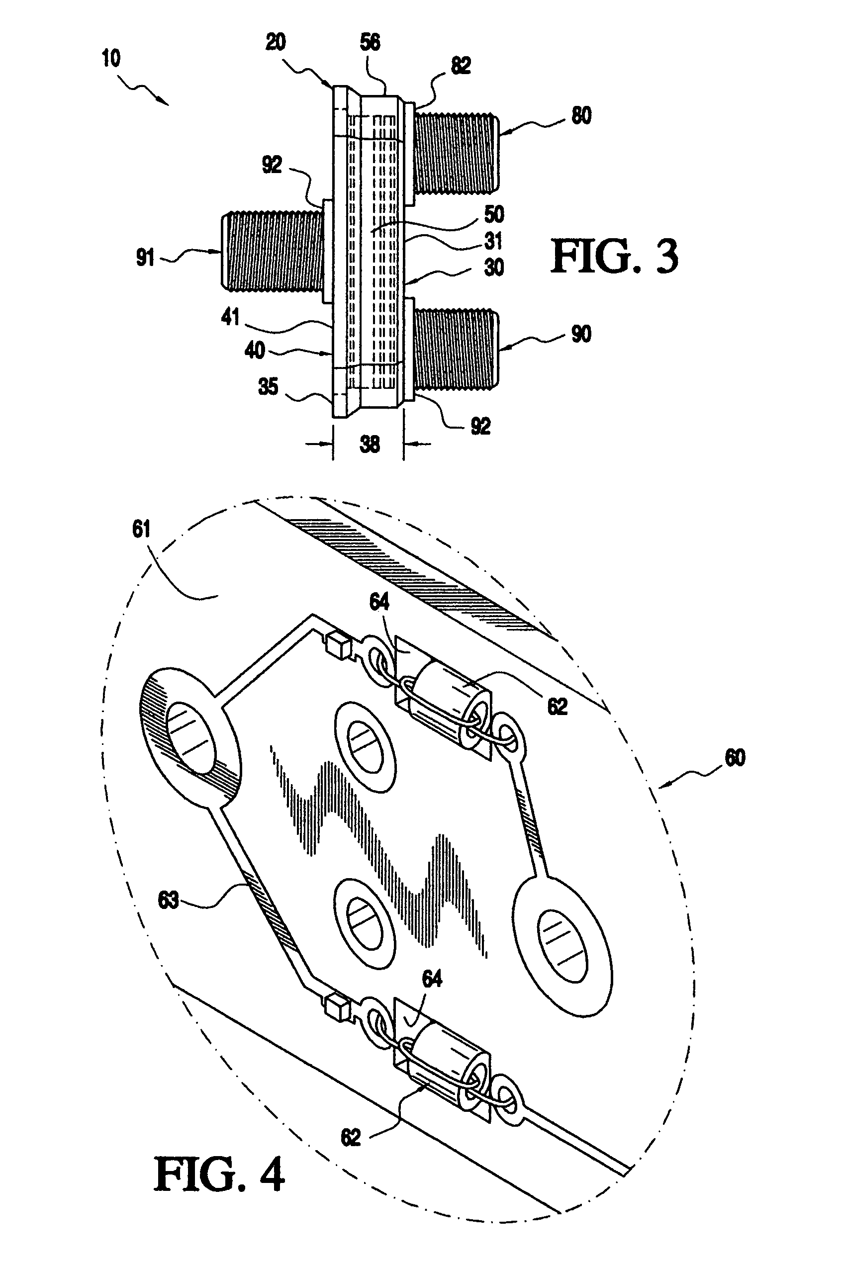
[0039] The present invention is an electronic signal continuity device 10, wherein the device 10 in particular is an electronic signal splitter. It should be appreciated that in other various exemplary embodiments the device could include other electronic continuity devices such as, but not limited to, directional couplers, multi-switches, and amplifiers for example.

[0040] The present invention incorporates a signal splitter / combiner with a single input connector and multiple “n” output connectors. The present invention utilizes current electronic signal splitting technology, such as but not limited to the basic “Wilkinson” technique on a printed circuit board or PCB. When the present invention is used as signal combiner, the multiple “n” output connectors become multiple “n” input connectors and the single input connector becomes the single output connector. Throughout this detailed description, only the aspects of the splitter will be discussed, with the understanding that when t...


PUM


Abstract

The present invention is an electronic signal continuity device comprising an electrically conductive case having a volume, an input port and at least two output ports. The continuity device further includes a printed circuit board (PCB) in electrical communication with the input port and the output ports. The PCB is operably configured to split an electronic signal received at the input port to the output ports. Additionally, the PCB is disposed within the volume of the electrically conductive case. Further, the PCB includes an orifice and a plurality of electronic components, wherein one of the plurality of electronic components is disposed in the orifice. The case further includes a first portion and a second portion opposing the first major portion, wherein one of the two output ports and the input port are disposed on the first portion, and one of the two output ports is disposed on the second portion.

Description

CROSS REFERENCE TO RELATED APPLICATION [0001] This nonprovisional application claims the benefit of Provisional Application No.: 60 / 690,208, filed on Jun. 13, 2005, which is incorporated herein by reference in its entirety and to which priority is claimed.BACKGROUND OF THE INVENTION [0002] 1. Field of Invention [0003] The present invention is related to the field of electronic signal splitter and combiners, in particular radio frequency splitters. [0004] 2. Description of Related Art [0005] Televisions and computers and other similar devices receive electronic signals from a variety of sources. The primary means to deliver electronic signals is through cables, predominately coaxial cables, which carry a signal from sources such as satellite receivers, land-line cable or roof mounted antennas. Many homes, apartments and offices today have multiple televisions and computers that used these signals. It is not the intent of this invention to discuss how an electronic signal is delivered...

Claims


Application Information

Patent Timeline
IPC IPC(8): H03H7/38
CPCH01R13/6658H01R2103/00H01R31/005H01R24/547
Inventor GALE, ROBERT D.
Owner GALE ROBERT D
Why Eureka
Try Eureka