Series fed amplified antenna reflect array

a reflect array and antenna technology, applied in the field of antennas, can solve the problems of narrow bandwidth of antennas, unsatisfactory methods of combining, and low power density of spatial arrays,

Inactive Publication Date: 2006-12-14
RAYTHEON CO
View PDF3 Cites 7 Cited by
  • Summary
  • Abstract
  • Description
  • Claims
  • Application Information

AI Technical Summary

Benefits of technology

[0021] The array is fabricated by via a metallization pattern which is disposed on a first substrate to provide a chip. The chip is secured to a second substrate with a bonding agent. In the best mode, the bonding agent is an anisotropic electrically conductive bonding film that allows current to flow along a path orthogonal to a surface of the array ...

Problems solved by technology

At millimeter wave frequencies, this method of combining typically produces unsatisfactory results due to heavy losses in the waveguide and/or microstrip medium.
However, spatial arrays have not yet produced the power density levels that are required for the more demanding applications mentioned above.
When integrated with the power-generating electronics on a thin semiconductor substrate, such antennas tend to have narrow bandwidths and high losses due to large surface currents.
The drawback of this...

Method used


Image

  • Series fed amplified antenna reflect array
  • Series fed amplified antenna reflect array
  • Series fed amplified antenna reflect array

Examples


Embodiment Construction

[0031] Illustrative embodiments and exemplary applications will now be described with reference to the accompanying drawings to disclose the advantageous teachings of the present invention.

[0032] While the present invention is described herein with reference to illustrative embodiments for particular applications, it should be understood that the invention is not limited thereto. Those having ordinary skill in the art and access to the teachings provided herein will recognize additional modifications, applications, and embodiments within the scope thereof and additional fields in which the present invention would be of significant utility.

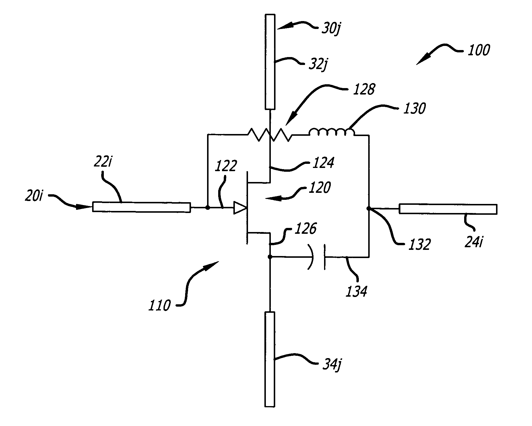
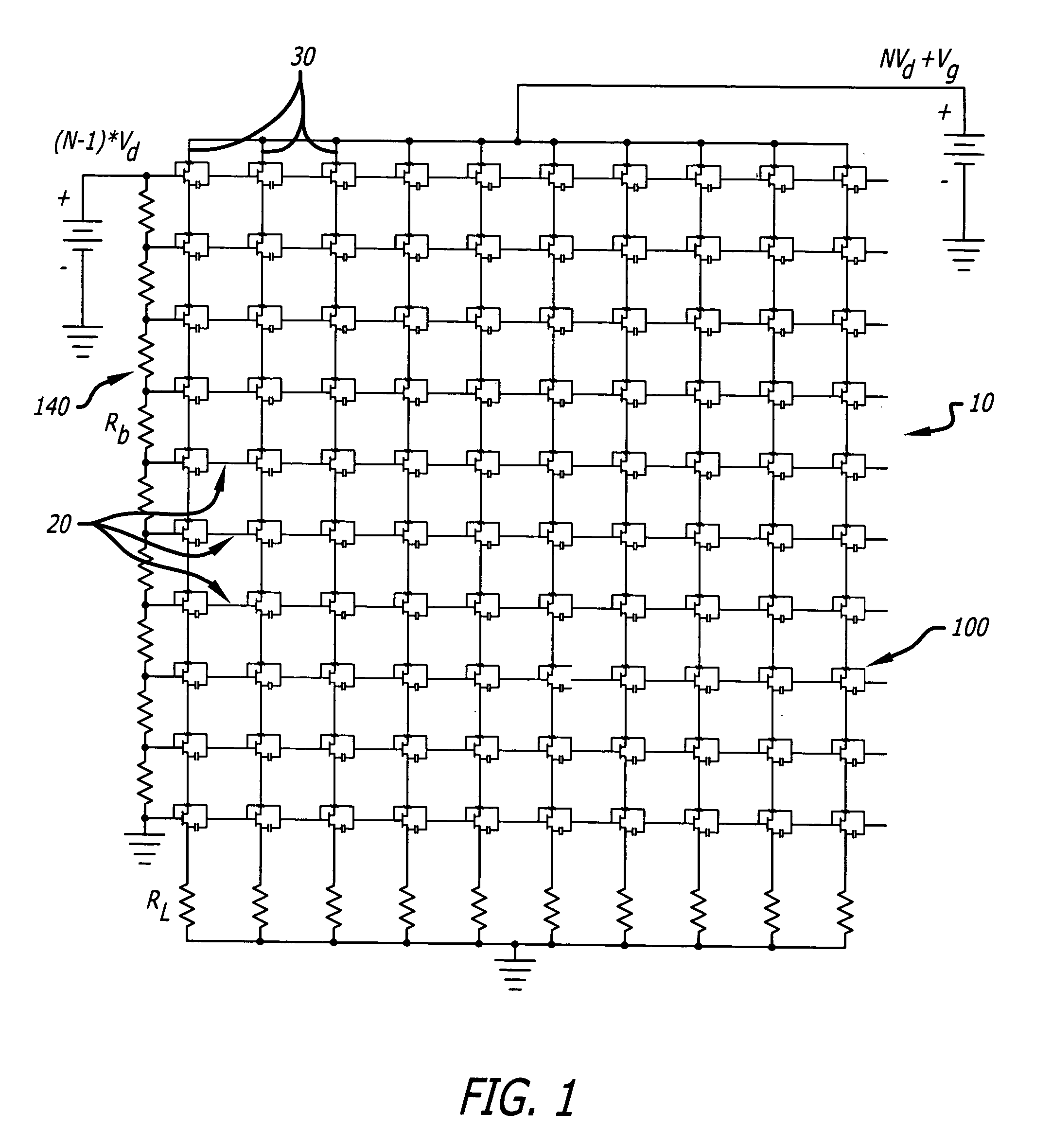
[0033]FIG. 1 is a schematic diagram of a series fed amplified reflect array 10 implemented in accordance with an illustrative embodiment of the present teachings.

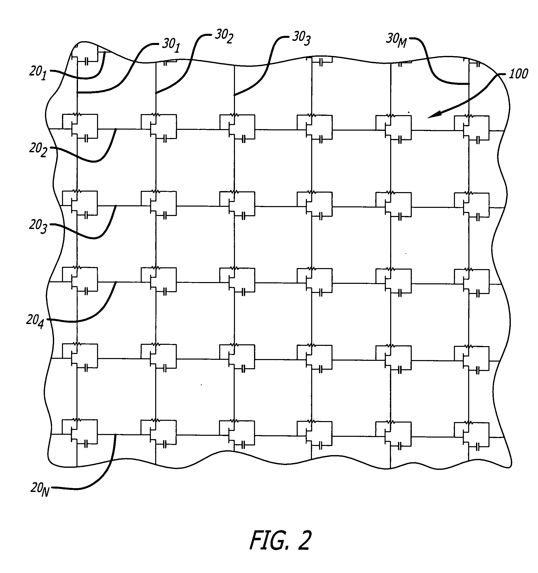
[0034]FIG. 2 is a magnified view a portion of the array 10 of FIG. 1. In the illustrative array implementation, the array includes N input dipole antennas 201, 202, 203, . . . 20N, wher...


PUM


Abstract

A reflect array antenna. The array includes a plurality of unit cells. Each cell includes a first dipole antenna having a first orientation and a first polarization; a second dipole antenna having a second orientation and a second polarization; and an amplifier input coupled inline to said first dipole antenna and output coupled inline to said second dipole antenna. The array further includes N first dipole antennas having a first orientation and a first polarization; M second dipole antennas having a second orientation and a second polarization; and a plurality of unit cells, each cell including an amplifier input coupled inline to a first dipole antenna and output coupled inline to a second dipole antenna. The second orientation and the second polarization are orthogonal to the first orientation and the first polarization. Each amplifier includes a transistor with an input terminal and first and second output terminals. Each input terminal is connected to the first dipole antenna and the output terminals are coupled to the second dipole antenna. The first and second terminals are adapted to be coupled to second and first terminals respectively of a neighboring cell in the array. A direct current bias for the array is applied via the second dipole antenna. Input bias for the transistors is applied via the first dipole antenna. A unique gate bias voltage for each transistor in the array is provided on a row-by-row basis via a voltage divider network. The voltage divider network includes (N−1) first resistors Rb connected in series to a first source of supply potential, where N is the number of rows in the array. Each of the resistors is connected to provide an input voltage to one of the transistors in the array. The resistive network further includes M second resistors RL connected to a respective one of the second dipoles antennas, where M is the number of columns in the array. The array is fabricated by via a metallization pattern which is disposed on a first substrate to provide a chip. The chip is secured to a second substrate with a bonding agent. In the best mode, the bonding agent is an anisotropic electrically conductive bonding film that allows current to flow along a path orthogonal to a surface of the array while blocking current flow parallel to the surface of the array.

Description

REFERENCE TO RELATED APPLICATION [0001] This is a continuation in part of U.S. patent application Ser. No. 10 / 153,140 filed May 20, 2002 by K. W. Brown et al. and entitled MONOLITHIC MILLIMETER WAVE REFLECTOR ARRAY SYSTEM (Atty. Docket No. PD 01W176) which issued Jul. 20, 2004 as U.S. Pat. No. 6,765,535 the teachings of which are hereby incorporated herein by reference and from which priority is hereby claimed.BACKGROUND OF THE INVENTION [0002] 1. Field of the Invention [0003] The present invention relates to antennas. More specifically, the present invention relates to millimeter wave reflect array antennas and arrays thereof. [0004] 2. Description of the Related Art [0005] As noted by the Institute of Electrical and Electronic Engineers (IEEE): “The millimeter-wave region of the electromagnetic spectrum is usually considered to be the range of wavelengths from 10 millimeters (0.4 inches) to 1 millimeter (0.04 inches). This means they are larger than infrared waves or x-rays, for e...

Claims


Application Information

Patent Timeline
IPC IPC(8): H01Q21/26H01Q9/28H01Q3/46H01Q21/06
CPCH01Q3/46H01Q21/061H03F3/604H03F2200/451H03F2200/18H03F2200/21H03F3/605
Inventor BROWN, KENNETH W.
Owner RAYTHEON CO
Why Eureka
Try Eureka