Bond method and structure using selective application of spin on glass

Active Publication Date: 2006-12-14
MIRADIA INC
View PDF16 Cites 26 Cited by
  • Summary
  • Abstract
  • Description
  • Claims
  • Application Information

AI Technical Summary

Benefits of technology

[0010] Many benefits are achieved by way of the present invention over conventional techniques. For example, the present technique provides an easy to use process that relies upon conventional technology. In some embodiments, the method provides higher device yields for the bonded substrates. Additionally, the method provides a process that is compatible with conventional process technology without substantial modifications to conventional equipment and processes. Preferably, the invention provides for an improved integrated structure including integrated circuits and mirror structures for display applications. In preferred embodiments, the present method provides a batch process, which can produce high throughput and yields. Moreover, device reliability is increased as a result of reduced outgassing and particle production. Additionally, the effects of thermal mismatch between materials are reduced through use of embodiments of the present inve

Problems solved by technology

Although very successful, CRTs were often bulky, difficult to make larger, and had other limitations.
Unfortunately, liquid crystal panels often had low yields and were difficult to scale up to larger sizes.
These LCDs were often unsuitable for larger displays often required for television sets and the lik

Method used


Image

  • Bond method and structure using selective application of spin on glass
  • Bond method and structure using selective application of spin on glass
  • Bond method and structure using selective application of spin on glass

Examples


Embodiment Construction

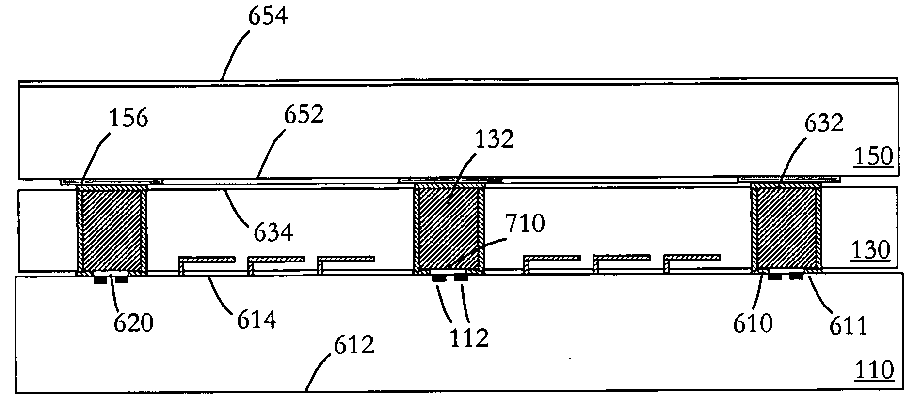
[0024] According to the present invention, techniques for packaging optical devices are provided. More particularly, the invention includes a method and structure for packaging optical devices using selective application of spin on glass for bonded substrates. Merely by way of example, the invention has been applied to integrating a mechanical based structure with an integrated circuit chip. But it would be recognized that the invention has a much broader range of applicability.

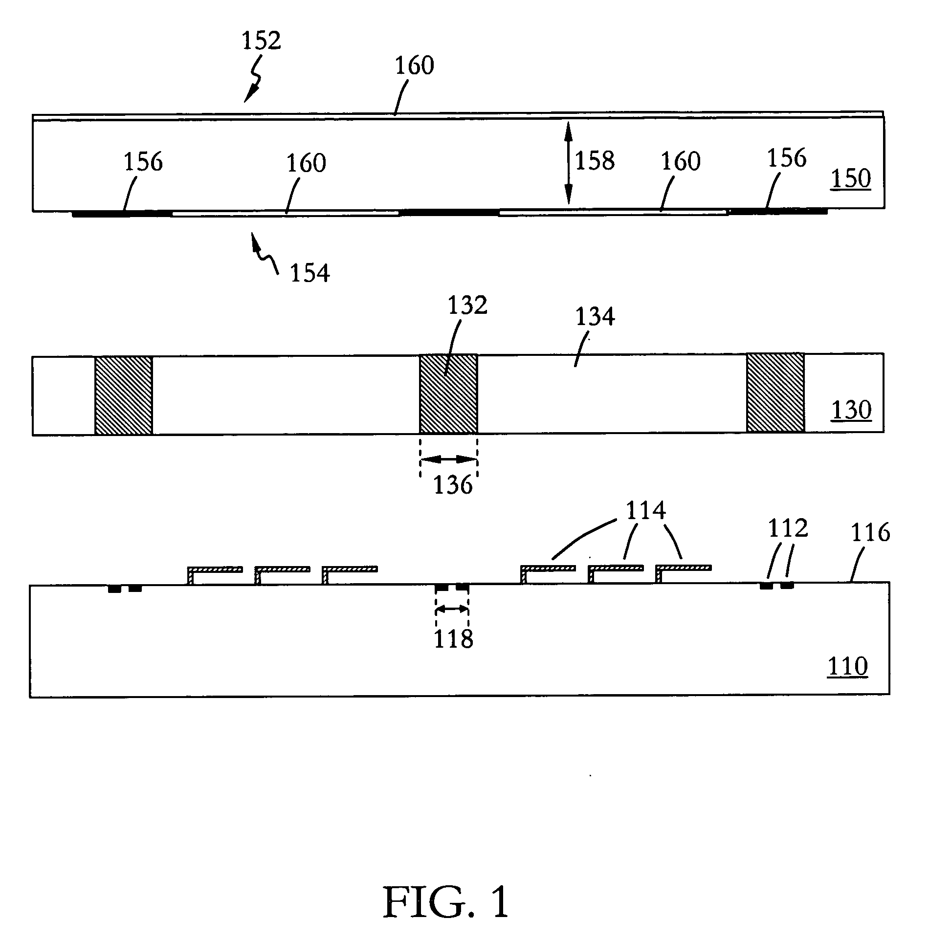
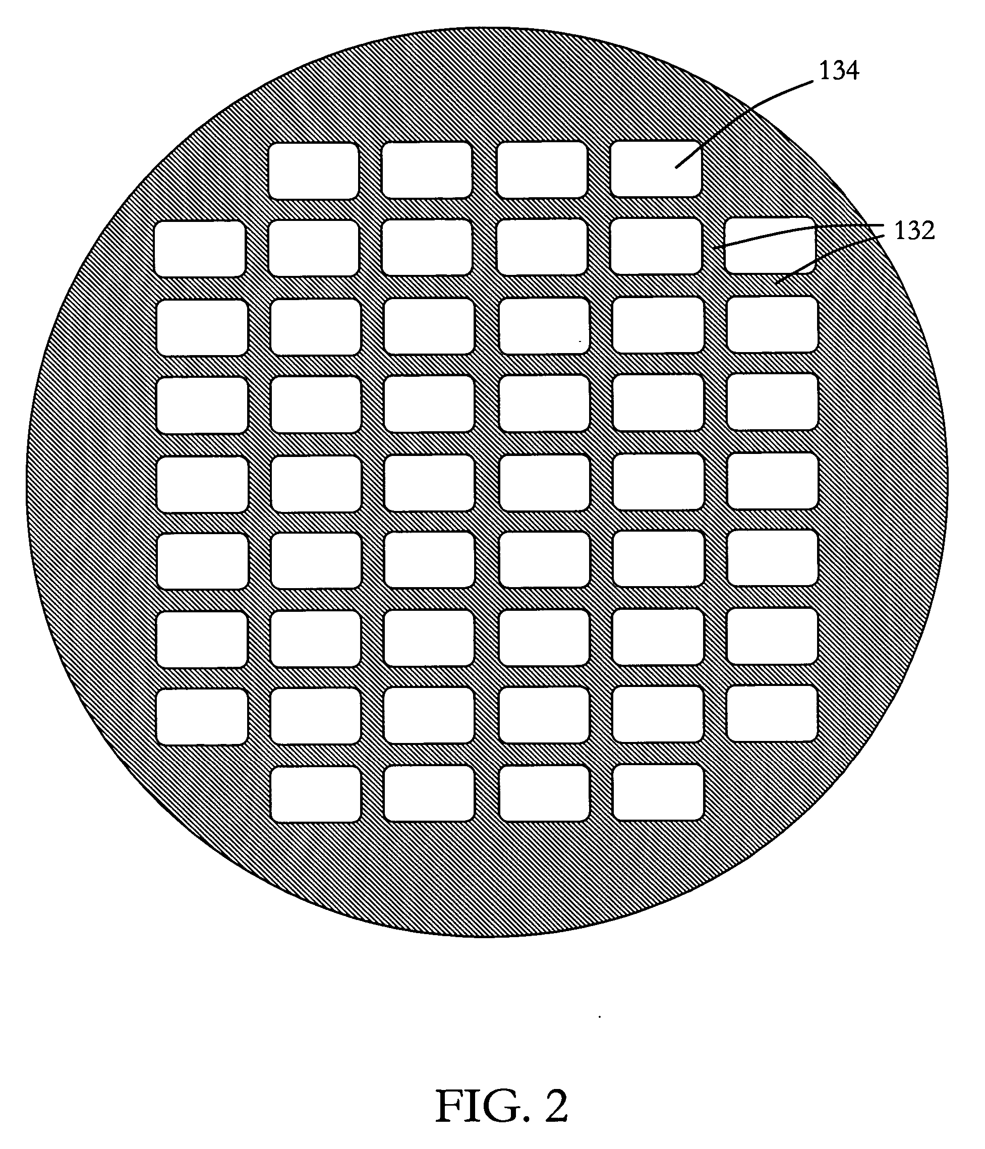
[0025]FIG. 1 is a simplified cross-sectional diagram illustrating components of a spatial light modulator (SLM) according to one embodiment of the present invention. The following diagrams are merely examples, which should not unduly limit the scope of the claims herein. One of ordinary skill in the art would recognize many variations, alternatives, and modifications. As illustrated in FIG. 1, a number of arrays of spatial light modulators are present on one surface of a CMOS substrate 110. As illustrated, a...


PUM


Abstract

A method for bonding substrate structures. The method includes providing a transparent substrate structure, the transparent substrate structure comprising a face region and an incident light region, providing a spacer structure, the spacer structure comprising a selected thickness of material, the spacer structure having a spacer face region and a spacer device region, and providing a device substrate structure, the device substrate having a device face region and a device backside region. The method further includes applying a first glue material to the spacer face region and bonding the spacer face region to the face region of the transparent substrate structure. The method also includes applying a second glue material to the spacer device region and bonding the spacer device region to the device face region.

Description

BACKGROUND OF THE INVENTION [0001] The present invention relates generally to packaging techniques. More particularly, the invention includes a method and structure for packaging optical devices using selective application of spin on glass for bonded substrates. Merely by way of example, the invention has been applied to integrating a mechanical based structure with an integrated circuit chip. But it would be recognized that the invention has a much broader range of applicability. [0002] Visual display technologies have rapidly developed over the years. Most particularly, electronic displays for outputting television shows, streaming video, and the like. From the early days, cathode ray tube technology, commonly called CRTs, outputted selected pixel elements onto a glass screen in conventional television sets. These television sets originally output black and white moving pictures. Color television sets soon replaced most if not all black and white television units. Although very su...

Claims


Application Information

Patent Timeline
IPC IPC(8): H01L21/00H01L21/30H01L23/12
CPCB81B7/0067H01L21/76251H01L21/316H01L21/02107
Inventor YANG, XIAO
Owner MIRADIA INC
Why Eureka
Try Eureka