Power detecting circuit and demodulator comprising it

a power detection circuit and demodulator technology, applied in the direction of pulse technique, frequency measurement arrangement, instruments, etc., can solve the problems of increasing production costs, conventional power detection circuits using schottky barrier diodes, and inconvenient integration of circuits, etc., to achieve excellent linearity of detection characteristics, low cost, and small variation of detection characteristics

Inactive Publication Date: 2006-12-21
SONY DEUT GMBH +1
View PDF1 Cites 11 Cited by
  • Summary
  • Abstract
  • Description
  • Claims
  • Application Information

AI Technical Summary

Benefits of technology

[0033] The present invention was made in consideration of the above circumstances and an object thereof is to provide a high-performance power detection circuit suitable to be made monolithic, formed a compact and low at cost, and suitable to a radio-frequency operation in a wide band, moreover, which has an excellent linearity of detection characteristics, exhibits a small variation of detection characteristics against a bias variation and small variation against FET threshold voltage variation, has a small DC offset, and does not require an additional circuit even when a subsequent stage circuit has a balanced input; and a demodulator using the same.

Problems solved by technology

The conventional power detection circuit using a Schottky barrier diode having the above characteristics suffers from the disadvantages below.
Accordingly, the conventional power detection circuit as above is not suitable to form an integrated circuit.
This results in the rising of production costs, limitation of an operation range and an increase of production variation.
When the above power detection circuit is configured in a semiconductor process capable of making an integrated circuit, the detection characteristic may be deteriorated.
However, the radio-frequency power detection circuit in FIG. 3 suffers from the disadvantages below.
Also, when the power detection circuit 2 has an output type of a single end type, and a subsequent stage of a linear detection circuit has a balanced input, an additional imbalance / balance conversion circuit becomes necessary.
Also, when the output type of the power detection circuit 3 is a single end type and a subsequent stage of a linear detection circuit thereof has a balanced input, an additional imbalance / balance conversion circuit is required.

Method used


Image

  • Power detecting circuit and demodulator comprising it
  • Power detecting circuit and demodulator comprising it
  • Power detecting circuit and demodulator comprising it

Examples


first embodiment

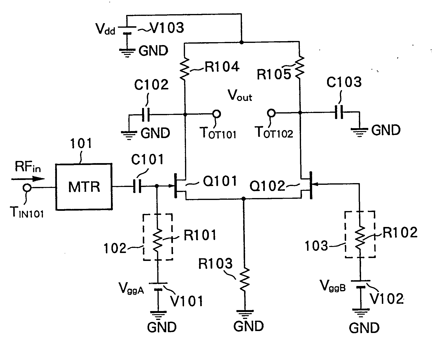
[0080]FIG. 7 is a circuit diagram showing a radio-frequency power detection circuit according to the present invention.

[0081] A radio-frequency power detection circuit 100 according to the first embodiment comprises first and second field-effect transistors (hereinafter, referred to as a transistor) Q101 and Q102 as two active elements, capacitors C101, C102, C103 and C104, resistor elements R101, R102, R103 R104 and R105, voltage sources V101, V102 and V103, and a matching circuit (MTR) 101.

[0082] A gate of the transistor Q101 is connected to one electrode of a DC cut capacitor C101, and the other electrode of the capacitor C101 is connected to an input terminal TIN101 for a radio-frequency signal RFin via the matching circuit 101.

[0083] Also, a gate of the transistor Q101 is connected to an end of the resistor element R101, and the other end of the resistor element R101 is connected to the voltage source V101 having a voltage of VggA. The resistor element R101 configures a first...

second embodiment

[0112]FIG. 10 is a circuit diagram showing a radio-frequency power detection circuit according to the present invention.

[0113] A different point in the second embodiment from the first embodiment explained above is that instead of connecting a resistor element as a current source between the connection point of sources of the transistors Q101 and Q102 and the ground potential GND, a transistor Q103 as a third FET having a gate supplied with a bias voltage from the third gate bias supply circuit 104, is connected.

[0114] The gate bias supply circuit 104 is configured by a resistor element R106 connected between a gate of the transistor Q104 and the voltage source V104 having a voltage of VggC.

[0115] The other configuration in the second embodiment is the same as that in the first embodiment.

[0116] According to the second embodiment, the same effects as in the first embodiment can be obtained.

third embodiment

[0117]FIG. 11 is a circuit diagram showing a radio-frequency power detection circuit according to the present invention.

[0118] The different points in the third embodiment to the first embodiment explained above are that instead of connecting the capacitors C102 and C103 between drains of the transistors Q101 and Q102 and the ground, a capacitor C105 (second capacitor) wherein the capacitance value is set to be a sufficiently large value so that the impedance becomes almost 0 ohm (Ω) in higher frequencies including an input radio-frequency signal Rfin is connected between a drain of the transistor Q101 and the drain of the transistor Q102.

[0119] The other configuration in the third embodiment is the same as that in the first embodiment.

[0120] According to the third embodiment, the same effects as in the first embodiment explained above are obtained, moreover, there are advantages that the number of parts can be reduced, and the fluctuation (variation) of drain potentials of the tr...


PUM


Abstract

A high performance power detection circuit suitable to be made monolithic, being compact and low at cost, suitable to a radio-frequency operation in a wide band, having excellent linearity in detection characteristics, small fluctuation of detection characteristics against bias fluctuation, small fluctuation of detection characteristics against FET threshold voltage fluctuation and a small DC offset, which does not require an additional circuit even when a subsequent circuit has a balanced input; and a demodulator using the same. The power detection circuit uses two transistors (FET) Q101 and Q102 having approximately same characteristics, wherein a connection point of sources are connected to a resistor element R103 as a current source, are used as active elements; gates and drains of the transistors Q101 and Q102 are supplied with approximately same bias voltages; drains of them are supplied with approximately same drain bias voltages; a capacitor C104, wherein a capacitance value is set to be a sufficiently large value, is connected between sources of transistors Q101 and Q102 and a ground; capacitors C102 and C103, wherein capacitance values are approximately same and set to be sufficiently large values, are connected between drains of the transistors Q101 and Q102 and a ground; a radio-frequency signal RFin is supplied to a gate of the transistor Q101; and a voltage difference between a drain of the transistor Q101 and a drain of the transistor Q102 is regarded as a detection output.

Description

TECHNICAL FIELD [0001] The present invention relates to a power detection circuit used in a communication apparatus for transmitting / receiving a radio-frequency signal and a measurement device for measuring a signal level of a radio-frequency signal, and a demodulator using the same. BACKGOUND ART [0002] In a conventional radio-frequency power detection circuit, mainly a Schottky barrier diode is often used. [0003]FIG. 1 is a circuit diagram showing a configuration of an example of a conventional radio-frequency power detection circuit using the diode. [0004] As shown in FIG. 1, the radio-frequency power detection circuit 1 comprises a diode D1 as an active element, a direct-current bias resistor element R1, a capacitor C1 and a load resistor element RL1. [0005] An anode of the diode D1 is connected to an input terminal Tin1 of a radio-frequency signal RFin and one end of the resistor element R1, and a cathode thereof is connected to an output terminal Tout1, one electrode of the ca...

Claims


Application Information

Patent Timeline
Patent Type & Authority Applications(United States)
IPC IPC(8): H03K9/06H03D1/18
CPCH03D1/18
Inventor ABE, MASAYOSHISASHO, NOBORUKRUPEZEVIC, DRAGANBRANKOVIC, VESELINRATNI, MOHAMED
Owner SONY DEUT GMBH
Why Eureka
Try Eureka