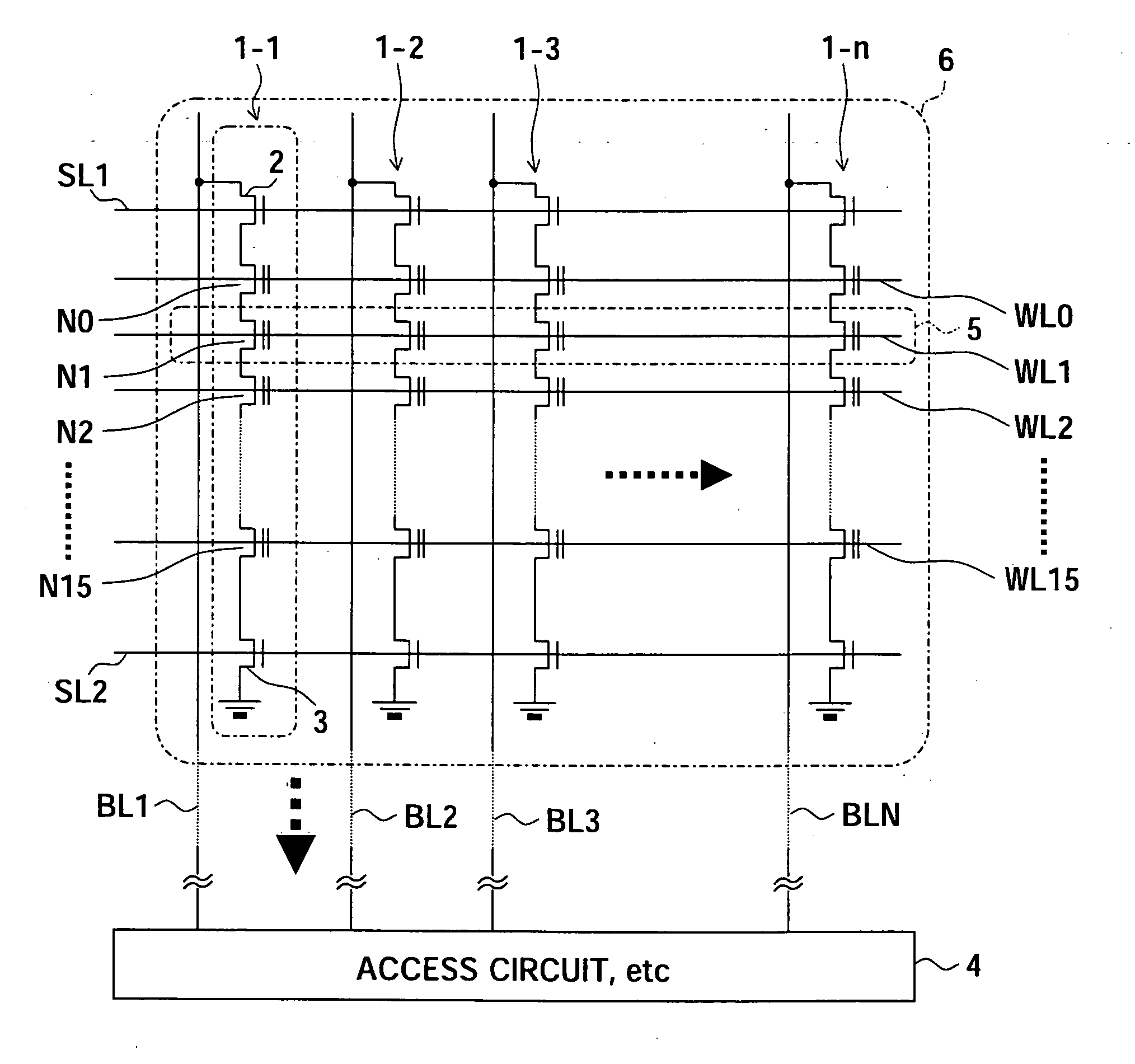
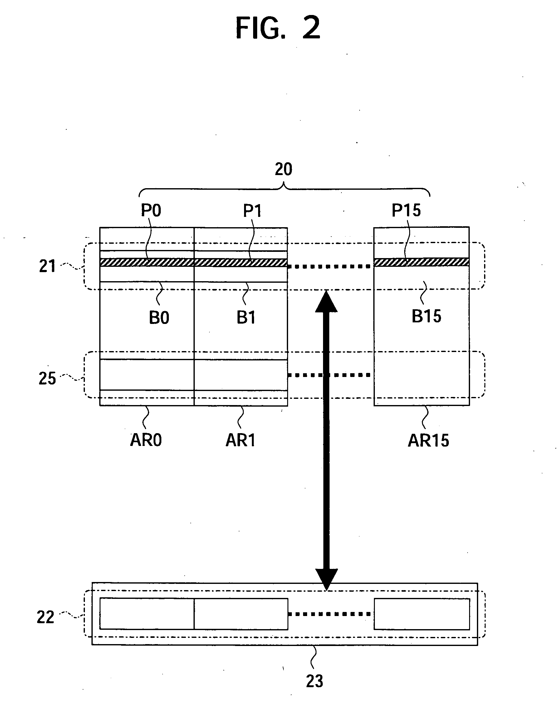
Storage device

Active Publication Date: 2006-12-21
SONY CORP
View PDF8 Cites 93 Cited by
  • Summary
  • Abstract
  • Description
  • Claims
  • Application Information

AI Technical Summary

Benefits of technology

[0017] In recent years, in order to overcome the limits of the size of the consumed power, the length of the seek time, the impact resistance, and the portability of hard disk drives, flash memories have been considered promising alternatives. However, as explained above, a flash memory cannot be increased in speed unless made large in access units. Further, data cannot be overwritten, so rewriting needs erasure and the erasure blocks at that time are even larg

Problems solved by technology

However, as explained above, a flash memory cannot be increased in speed unless made large in access units.
Further, data cannot be overwritten,

Method used


Image

  • Storage device
  • Storage device
  • Storage device

Examples


first embodiment

[0066]FIG. 3 is a view of a configuration showing a storage device according to the present invention.

[0067] A storage device 30 of FIG. 3 has an interface circuit (I / F) 31, a page buffer 32, an internal data bus 33, a transfer control circuit 34, and NAND type flash memories 35 and 36 as principal components.

[0068] In the storage device 30, the 32-bit internal data bus 33 has two chips constituted by NAND type flash memories 35 and 36 having 16-bit input / outputs connected to it in parallel. The two NAND type flash memories 35 and 36 are simultaneously accessed in parallel in a read operation and a write operation. The page buffer 32 temporarily stores the accessed page data via the internal data bus 33 and is connected to the interface circuit 31 with the outside. The transfer control circuit 34 manages the transfer between the two flash memories 35 and 36 and the page buffer 32. The transfer control circuit 34 has a built-in RAM 37. The built-in RAM 37 has an address conversion t...

third embodiment

[0089] Such hierarchical arrangement of virtual addresses makes flexible management possible even for a parallel configuration of a plurality of chips or a plurality of banks. FIG. 8 shows a third embodiment using two chips configured in parallel.

[0090]FIG. 8 is a view of a configuration showing a storage device according to a third embodiment of the present invention. FIGS. 9A and 9B are diagrams showing an example of the configuration of the address conversion table in the transfer control circuit according to the third embodiment of the present invention.

[0091] In a storage device 30D according to the third embodiment, two chips of flash memories of the second embodiment are arranged in parallel. Physical address fields PBA0 and PBA1 in the erasure block unit address conversion table 51d are independently arranged for the chips of the flash memories 35d and 36d. Namely, in a RAM 50d built-in the transfer control circuit 34d, substantially two sets of erasure block unit address c...

second embodiment

[0106] An address conversion table 38h stored in a RAM 37c is the same as that of the present invention. Note that a RAM 50c stores a table 51h indicating the state of defects for each physical block address PBA and the state of usage of the blocks. The defect flag DEF indicates a defect in the target block. On the other hand, the usage flag USD becomes “0” after erasing the block and becomes “1” when data is written into even one portion. Further, a write pointer indicating the previously written page address is stored in a register 53h. The usual write operation is executed in a form of incrementing the pointer. Namely, in the same block, the data are sequentially written from the page address “0x00” toward “0xFF”.

[0107] In the present embodiment, when writing in a flash memory, the physical page address for the writing is determined from the table 51h and the register 53h. At this time, any defect block from which defect information is detected is skipped, whereby pages in the de...


PUM


Abstract

A storage device, enabling elimination of redundant write operations of non-selected data and enabling optimization of arrangement of pages to a state efficient for rewriting, having two flash memories which can be accessed in parallel, a page register for acquiring data in parallel from the flash memories and temporarily storing the same, and a control circuit having a built-in RAM in which is constructed an address conversion table for managing correspondence between logical addresses and physical addresses in units of data stored in parallel in the page register, wherein data is rewritten by updating of the address conversion table and additional writing into a storage medium.

Description

CROSS REFERENCES TO RELATED APPLICATIONS [0001] The present invention contains subject matter related to Japanese Patent Application No. 2005-165234 filed in the Japan Patent Office on Jun. 6, 2005, and Japanese Patent Application No. 2006-115779 filed in the Japan Patent Office on Apr. 19, 2006 the entire contents of which being incorporated herein by reference. BACKGROUND OF THE INVENTION [0002] 1. Field of the Invention [0003] The present invention relates to a storage device including a non-volatile memory, more particularly relates to a speed-up of data transfer in a storage device including a flash memory. [0004] 2. Description of the Art [0005] In recent years, flash memories have been attracting attention as storage media of digital still cameras and mobile computer equipment. [0006] A flash memory is a semiconductor memory using tunneling or hot electron acceleration to make electrons pass through a gate insulation film and injecting these into a floating gate or a trap lay...

Claims


Application Information

Patent Timeline
IPC IPC(8): G11C16/04G11C11/34
CPCG06F3/061G06F3/0662G11C16/102G06F12/0246G06F2212/7201G06F3/0679G06F12/02
Inventor NISHIHARA, TOSHIYUKIISHIMOTO, TAKESHI
Owner SONY CORP
Why Eureka
Try Eureka