Semiconductor device

a technology of semiconductor devices and semiconductors, applied in the direction of electric digital data processing, digital storage, instruments, etc., can solve the problems of unrighteous reading of program contents, possible failure of operation or human suffering, security holes, etc., and achieve the effect of high data confidentiality protection function, not lowering processing speed, and simple processing

Active Publication Date: 2006-12-21
RENESAS ELECTRONICS CORP
View PDF3 Cites 13 Cited by
  • Summary
  • Abstract
  • Description
  • Claims
  • Application Information

AI Technical Summary

Benefits of technology

[0017] The present invention was made to solve the above-described problem, and a first object thereof is to provide a semiconduct

Problems solved by technology

When a user of a microcomputer including the non-volatile memory (hereinafter also referred to as an end user) as such should rewrite the program stored therein, operation failure or human suffering might possibly occur.
There is also a concern that a competitor may unrighteously read the contents of the program.
Presence of such an arrangement itself, however, may be a security hole.
Specifically, if an ill-intentioned third party should scrutinize the microcomputer and find the specific signal or the specific ID, the protection function would be lost.
Microcomputers come to have higher performances recently, and programs for operating the microcomputers come to be l

Method used


Image

  • Semiconductor device
  • Semiconductor device
  • Semiconductor device

Examples


embodiment 1

[0037] Embodiment 1 is directed to a protection function proposed for an IP vendor or a programmer considering protection against an end user.

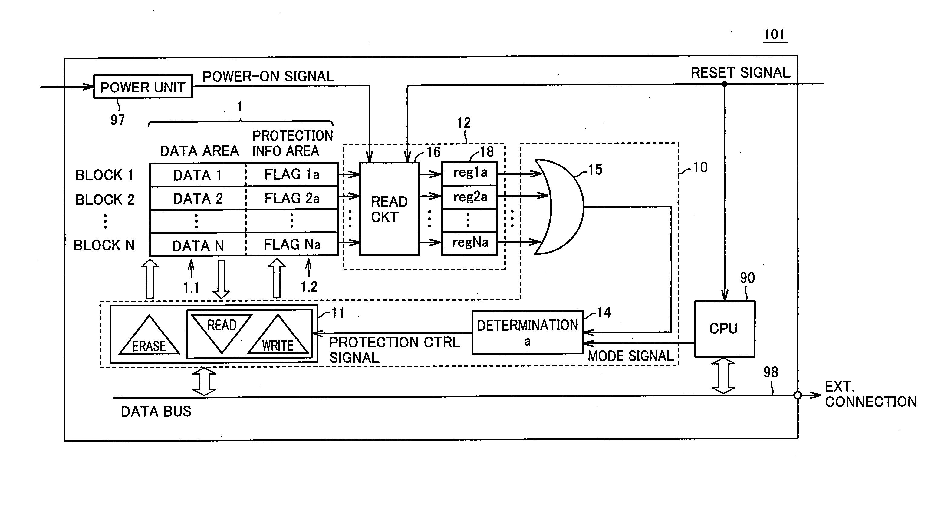
[0038] Referring to FIG. 1, a semiconductor device 101 in accordance with Embodiment 1 includes a data bus 98, an operating unit (CPU: Central Processing Unit; hereinafter also denoted by “CPU”) 90, a non-volatile memory 1, a reading unit 12, a control unit 10 and a power unit 97.

[0039] Data bus 98 connects CPU 90, control unit 10, an external memory (not shown) and an external device (not shown) to each other, mediating data exchange.

[0040] CPU 90 passes data to / from non-volatile memory 1 through data bus 98. Receiving a reset signal from the outside, CPU 90 reads a program stored in non-volatile memory 1 or an external memory (not shown) to be activated, in accordance with an operation mode, as will be described later. Further, when CPU 90 reads a program from non-volatile memory 1 to be activated, it outputs a mode signal thereof to cont...

embodiment 2

[0070] In Embodiment 1, a semiconductor device having a protection function proposed for an IP vendor or a programmer considering protection against an end user has been described.

[0071] In Embodiment 2, a semiconductor device having a protection function proposed for an IP vendor considering protection against a programmer or an end user will be described.

[0072] Referring to FIG. 3, a semiconductor device 102 in accordance with Embodiment 2 includes a data bus 98, a CPU 92, a non-volatile memory 2, a reading unit 22, a control unit 20 and a power unit 97.

[0073] Data bus 98 connects CPU 92, control unit 20, an external memory (not shown) and an external device (not shown) to each other, mediating data exchange.

[0074] CPU 92 passes data to / from non-volatile memory 2 through data bus 98. Similar to CPU 90 in accordance with Embodiment 1, when CPU 92 reads a program from non-volatile memory 2 to be activated (in the “activation mode on a program in a memory of the microcomputer”), ...

embodiment 3

[0095] In Embodiments 1 and 2, protection functions directed to different objects have been described.

[0096] In Embodiment 3, a semiconductor device that can simultaneously realize functions of Embodiments 1 and 2 will be described. In the following description, for clarification, the protection in accordance with Embodiment 1 is also referred to as “overall protection,” and protection in accordance with Embodiment 2 is also referred to as “partial protection.”Referring to FIG. 4, a semiconductor device 103 in accordance with Embodiment 3 includes a data bus 98, a CPU 92, a non-volatile memory 3, a reading unit 32, a control unit 30 and a power unit 97.

[0097] Data bus 98 connects CPU 92, control unit 30, an external memory (not shown) and an external device (not shown) to each other, mediating data exchange.

[0098] CPU 92 passes data to / from non-volatile memory 3 through data bus 98. Similar to CPU 90 in accordance with Embodiment 1, when CPU 92 reads a program from non-volatile m...


PUM


Abstract

Receiving a request for canceling setting, a control circuit erases data stored in a corresponding block, changes a value of a protection flag, and cancels protection setting. When an overall protection is set for any block, the control circuit prohibits access to all blocks, except when it is an operation mode for activating a memory program contained in the microcomputer. Further, control circuit permits an access to a block M only when partial protection is set, CPU is in the mode for activating a memory program contained in the microcomputer and the access is for reading an instruction code in accordance with an instruction fetch.

Description

BACKGROUND OF THE INVENTION [0001] 1. Field of the Invention [0002] The present invention relates to a semiconductor device including a non-volatile storage unit and, more specifically, to a semiconductor device with data confidentiality protecting function. [0003] 2. Description of the Background Art [0004] Conventionally, microcomputers used for various purposes generally include a non-volatile storage unit (hereinafter also referred to as a non-volatile memory) such as a flash memory or an EEPROM (Electrically Erasable and Programmable Read Only Memory). When data is once written, a non-volatile memory retains the data even when the power is turned off, and it allows free rewriting of data. Therefore, a microcomputer embedded in a product with a program stored in a non-volatile memory advantageously allows a so-called updating, including program modification or addition of a new function. [0005] When a user of a microcomputer including the non-volatile memory (hereinafter also re...

Claims


Application Information

Patent Timeline
IPC IPC(8): G11C16/04G06F21/60G06F21/62G06F21/79
CPCG06F21/79G11C16/22G06F2221/2143
Inventor KUROSAWA, HITOSHI
Owner RENESAS ELECTRONICS CORP
Why Eureka
Try Eureka