

Semiconductor laser device having an insulation region
a semiconductor laser and insulation region technology, applied in semiconductor lasers, laser details, active medium materials, etc., can solve the problems of reducing the fabrication time to yield of the semiconductor laser with grating correspondingly, the purpose of tuning the output optical wavelength cannot be achieved, and the fabrication process to fabricate the semiconductor laser device is simplified. , the effect of low fabrication cos
- Summary
- Abstract
- Description
- Claims
- Application Information
AI Technical Summary
Benefits of technology
Problems solved by technology
Method used
Image

Examples
Embodiment Construction
[0027] The following description contains specific information pertaining to the implementation of the present invention. One skilled in the art will readily recognize other advantages and features of the present invention after reviewing what specifically disclosed in the present application. It is manifest that the present invention can be implemented and applied in a manner different from that specifically discussed in the present application. It should also be understood that the invention is not limited to the particular exemplary embodiments described herein, but is capable of many rearrangements, modifications, and substitutions without departing from the spirit of the present invention.
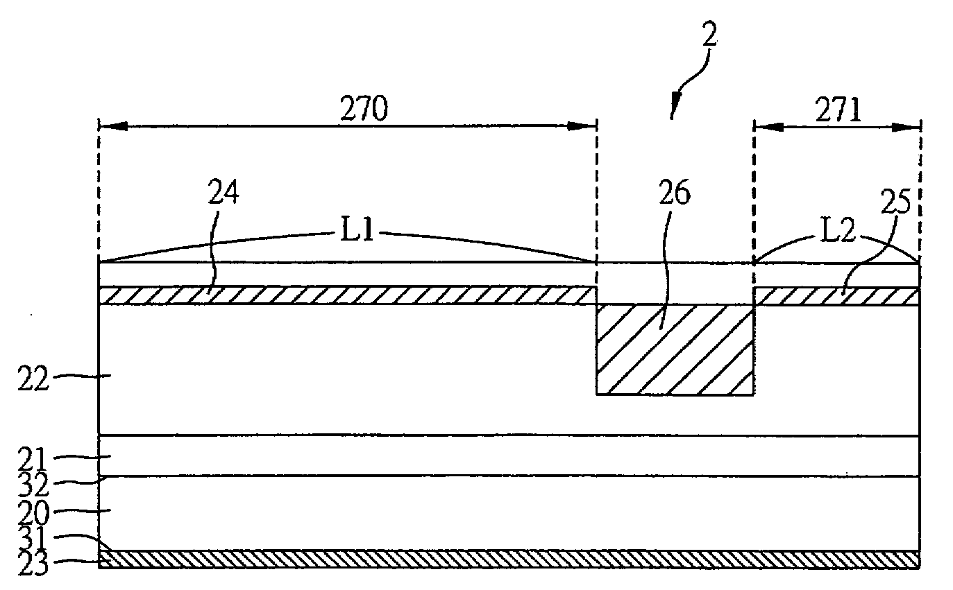
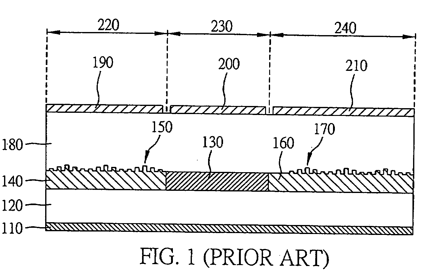
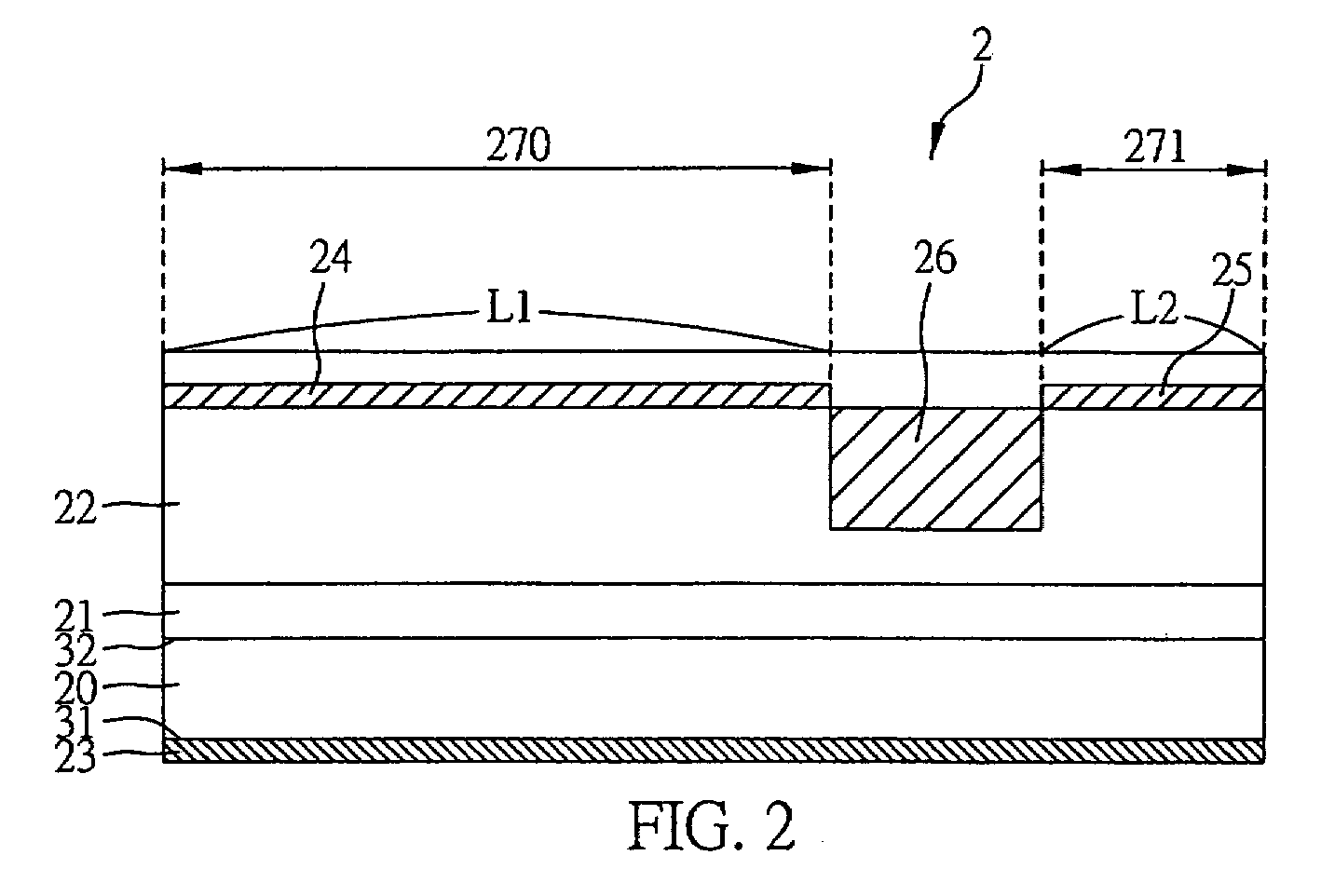
[0028]FIG. 2 is a cross-sectional view of a semiconductor laser device 2 of the preferred embodiment according to the present invention. Please note that the drawings are all simplified schematic diagrams and merely illustrate the basic structure according to the present invention should be p...
PUM
 Abstract
Description
Claims
Application Information