Method for chemical vapor deposition in high aspect ratio spaces

Active Publication Date: 2006-12-28
RGT UNIV OF CALIFORNIA
View PDF4 Cites 1 Cited by
  • Summary
  • Abstract
  • Description
  • Claims
  • Application Information

AI Technical Summary

Benefits of technology

[0009] In one aspect of the invention, a CVD-based process for filling high aspect ratio spaces in a substrate includes the step of forming a gradient of precursor gas inside the space(s) prior to deposition. The gradient may be formed, for example, by first filling a deposition chamber with the reactant gas at high pressure, followed by reducing the pressure within the deposition chamber or by partial evacuation of the deposition chamber. The temperature of the substrate is then briefly increased to preferentially deposit precursor material within the “deep” portion of the high aspect ratio space. The process may be repeated for a number of cycles to completely fill the space(s). The process permits the filling of high aspect ratio spaces without any voids or keyholes that may adversely impact the performance of the resulting device.

Problems solved by technology

Many semiconductor devices include, for example, vias, gaps, trenches or other structures that contain large aspect ratios that present unique deposition process challenges.
One such problem arises when a space having a large aspect ratio is filled using chemical vapor deposition (CVD) techniques.
Consequently, the deposited layer nearer the opening of the trench closes or pinches, creating voids or spaces that are left unfilled.
The voids left in semiconductor devices pose a significant problem.
For example, voids may result in failure of the device caused by gases (or other materials) contained in the voids.
In addition, it is possible that voids may be filled with conductive material during subsequent deposition processes thereby causing shorts in the device components.

Method used


Image

  • Method for chemical vapor deposition in high aspect ratio spaces
  • Method for chemical vapor deposition in high aspect ratio spaces
  • Method for chemical vapor deposition in high aspect ratio spaces

Examples


Embodiment Construction

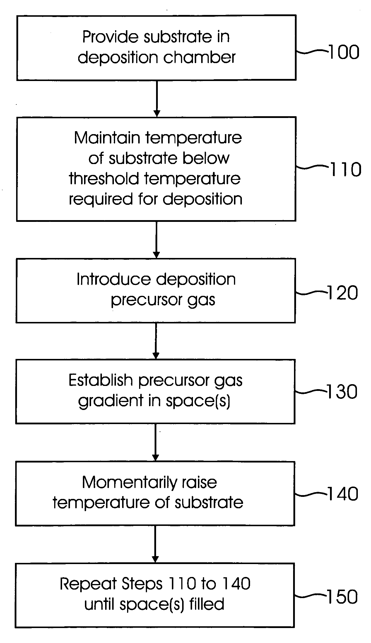
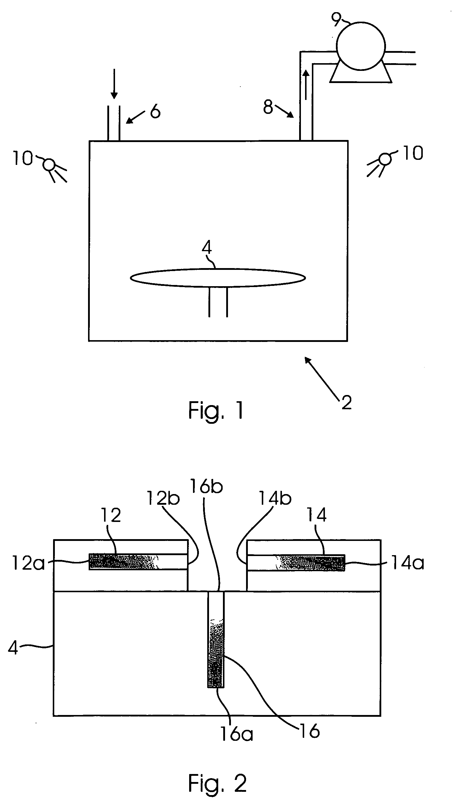
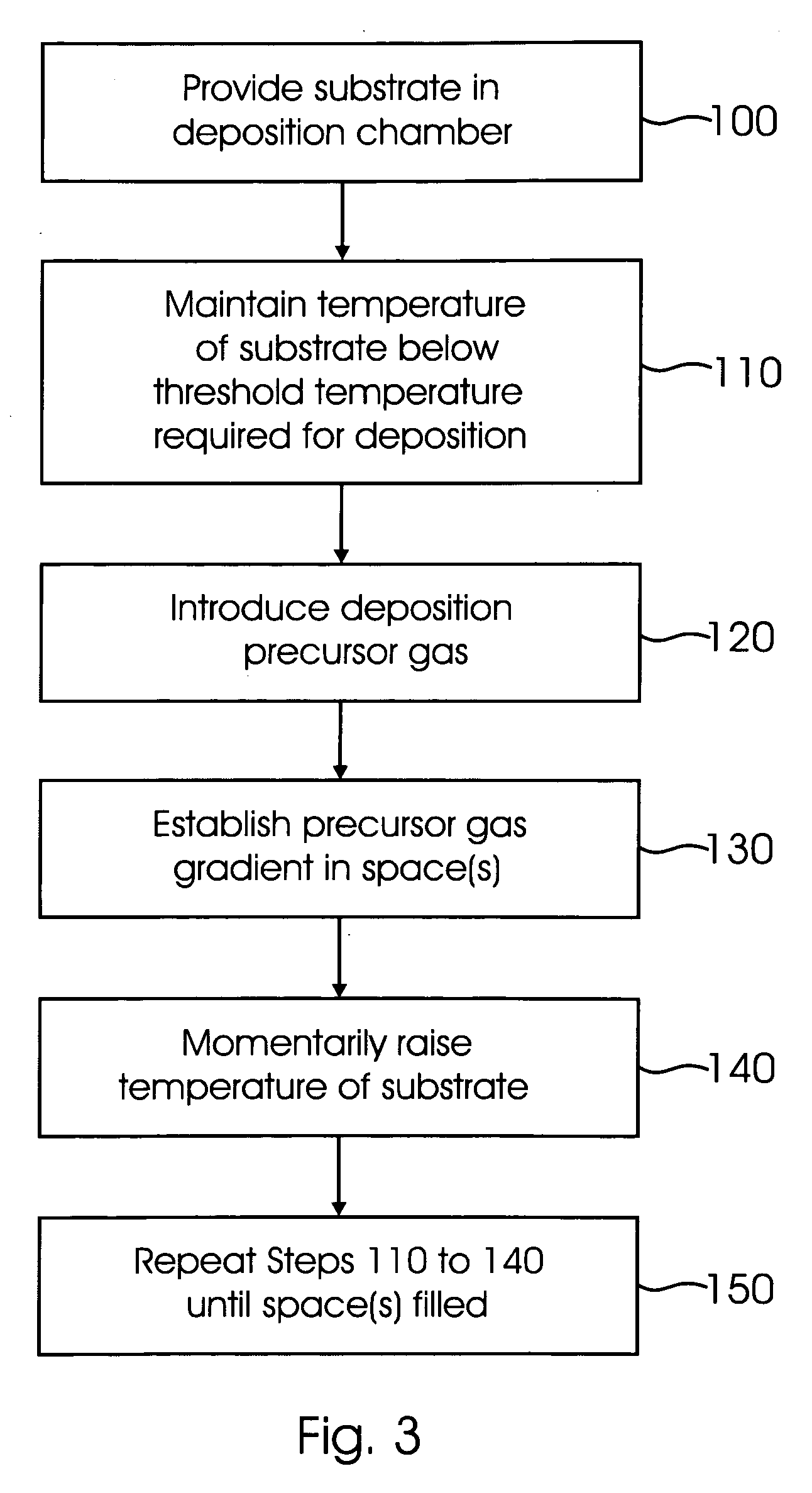
[0020]FIG. 1 illustrates a deposition chamber 2 used for chemical vapor deposition of conformal films. The deposition chamber 2 may be a chamber used, for example, in low pressure chemical vapor deposition (LPCVD) and / or rapid temperature chemical vapor deposition (RTCVD). The deposition chamber 2 is preferably able to rapidly change pressure in response to a user input or control algorithm. The deposition chamber 2 illustrated in FIG. 1 includes a substrate 4 therein. Of course, multiple substrates 4 may be located inside the deposition chamber 2. The substrate 4 may comprise substrate material commonly used in integrated circuit technology and / or MEMS devices. The substrate 4 may comprise silicon or other semiconductor material. The substrate 4 may include active regions that need to be separated or otherwise isolated from one another, e.g., transistors separated by trenches or other isolation structures.

[0021] The deposition chamber 2 preferably includes one or more inlets 6 and...


PUM

PropertyMeasurementUnit
Thicknessaaaaaaaaaa
Thicknessaaaaaaaaaa
Thicknessaaaaaaaaaa

Abstract

A method of depositing conformal film into high aspect ratio spaces includes the step of forming a gradient of precursor gas inside the space(s) prior to deposition. The gradient may be formed, for example, by reducing the pressure within the deposition chamber or by partial evacuation of the deposition chamber. The temperature of the substrate is then briefly increased to preferentially deposit precursor material within the closed or “deep” portion of the high aspect ratio space. The process may be repeated for a number of cycles to completely fill the space(s). The process permits the filling of high aspect ratio spaces without any voids or keyholes that may adversely impact the performance of the resulting device.

Description

FIELD OF THE INVENTION [0001] The field of the invention generally relates to methods of depositing conformal films on substrates. In particular, the field of the invention relates to methods of depositing conformal films on or into high aspect ratio spaces such as, for example, gaps, vias and trenches. BACKGROUND OF THE INVENTION [0002] The semiconductor industry is increasingly being driven to decrease the size of semiconductor devices located on integrated circuits. For example, miniaturization is needed to accommodate the increasing density of circuits necessary for today's semiconductor products. The rapid advancement of silicon-based integrated circuit technology brings along the increasingly stringent requirement on the ability of depositing film into spaces having high aspect ratios, e.g. spaces where the ratio of the longest dimension to the shortest dimension is greater than 10. Many semiconductor devices include, for example, vias, gaps, trenches or other structures that ...

Claims


Application Information

Patent Timeline
IPC IPC(8): H01L21/31
CPCH01L21/02271H01L21/28556H01L21/31604C23C16/481H01L21/76877C23C16/045C23C16/45557H01L21/76843H01L21/31C23C16/00
Inventor XIE, YA-HONG
Owner RGT UNIV OF CALIFORNIA
Why Eureka
Try Eureka