Method for producing dislocation-free strained crystalline films

a crystalline film, dislocation-free technology, applied in the direction of basic electric elements, semiconductor/solid-state device manufacturing, electric devices, etc., can solve problems such as affecting the overall performance of the device, and achieve the effect of small thickness

Active Publication Date: 2006-12-28
RGT UNIV OF CALIFORNIA
View PDF14 Cites 114 Cited by
  • Summary
  • Abstract
  • Description
  • Claims
  • Application Information

AI Technical Summary

Benefits of technology

[0011] In one aspect of the process described above, the silicon dioxide layer on the back side of the first substrate is patterned. In another aspect of the process, the second substrate has a smaller thickness than the first substrate. The degree of curvature of the second substrate may be greater than the degree of curvature of the first substrate.

Problems solved by technology

Dislocations that are formed in strained silicon (particularly threading dislocations), however, impair the overall performance of the device.

Method used


Image

  • Method for producing dislocation-free strained crystalline films
  • Method for producing dislocation-free strained crystalline films
  • Method for producing dislocation-free strained crystalline films

Examples


Embodiment Construction

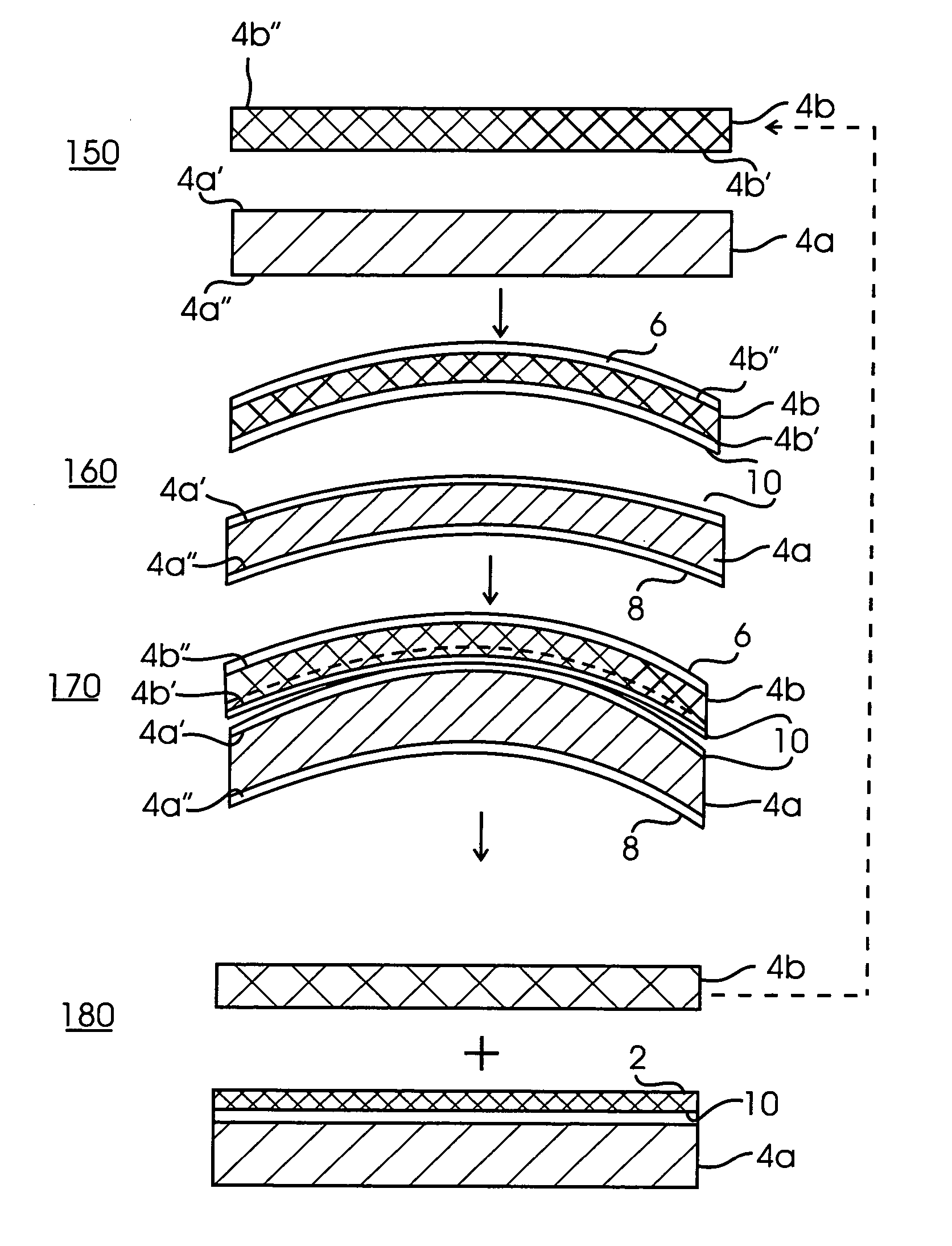
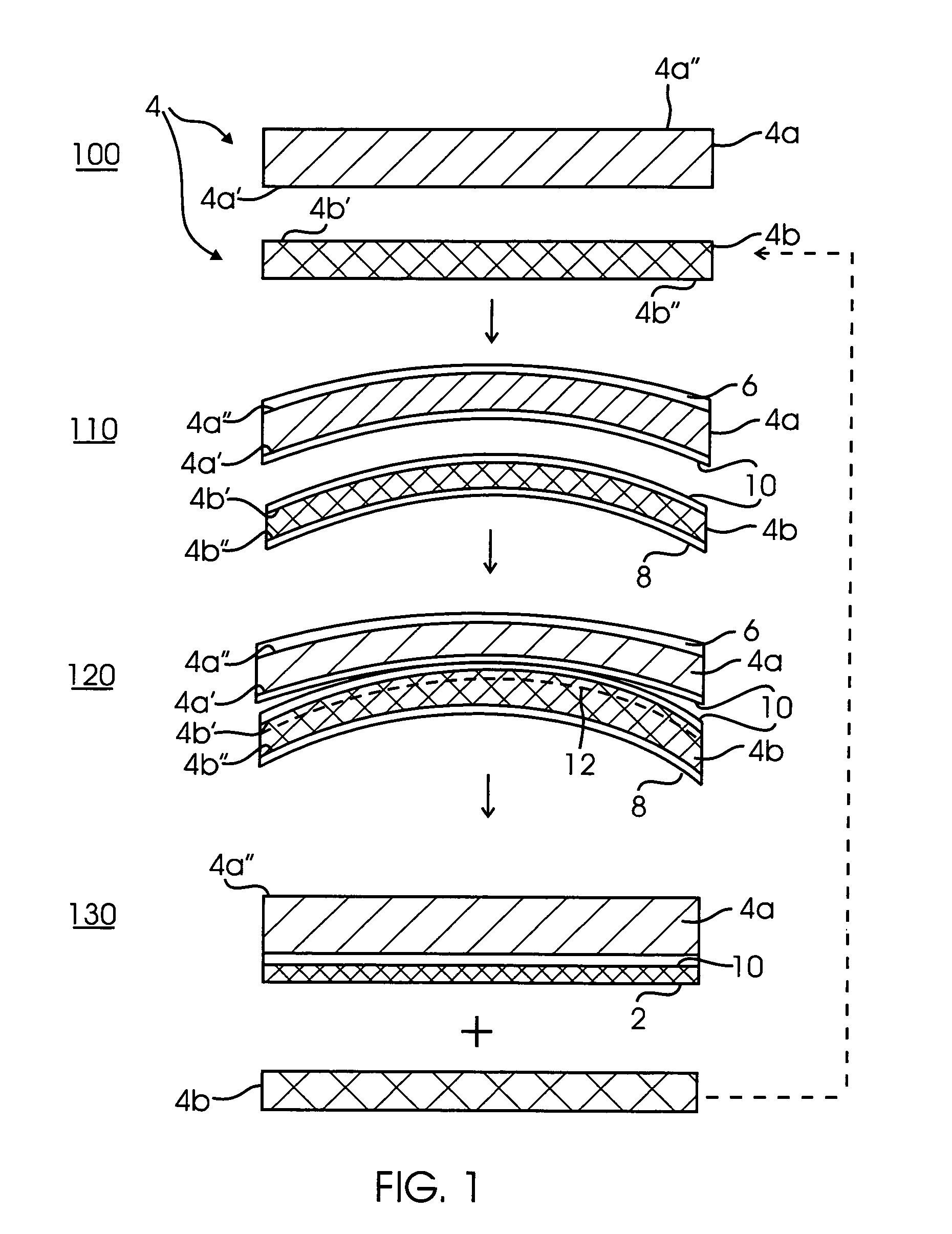
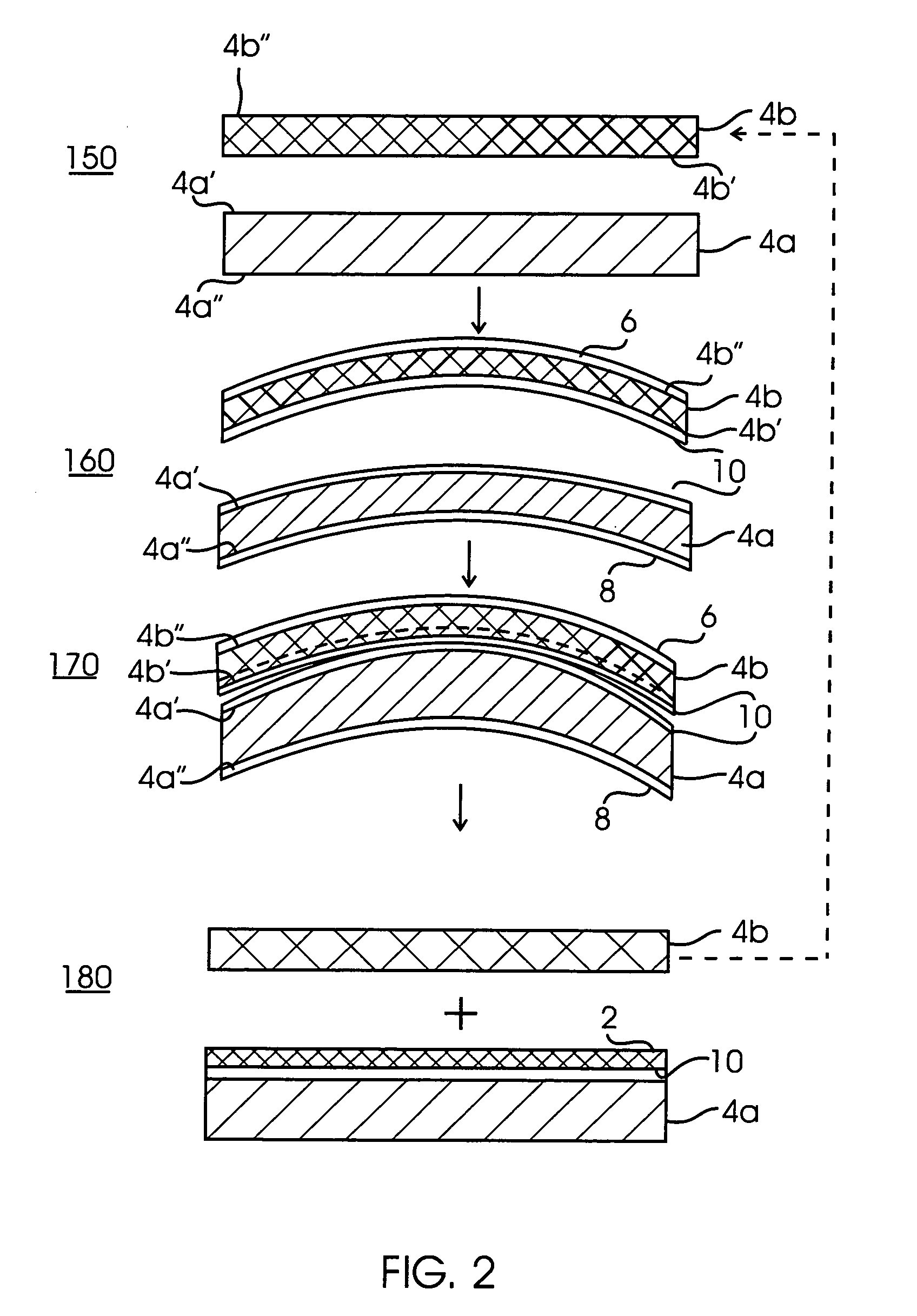
[0022]FIGS. 1 and 2 illustrate two methods for forming a dislocation-free strained silicon thin film 2 on a substrate 4. FIG. 1 illustrates a process for making a tensile-strained silicon thin film 2 while FIG. 2 illustrates a process for making compressively-strained silicon thin film 2. A key advantage of the process described herein is that there are substantially no dislocations formed in the thin film 2. Consequently, the strained film 2 is completely free of dislocations (e.g., threading dislocations) and is very homogeneous. The improved properties of the resultant strained thin film 2 make it particularly useful for incorporation into semiconductor-based devices.

[0023] With reference now to FIG. 1, the process begins (step 100 in FIG. 1) by providing a first substrate 4a and a second substrate 4b. The first and second substrates 4a, 4b may comprise, for example, a silicon substrate in the form of a wafer or the like. Of course other materials other than silicon may be used ...


PUM


Abstract

A method for forming dislocation-free strained silicon thin film includes the step of providing two curved silicon substrates. One substrate is curved by the presence of silicon dioxide on a back surface. The other substrate is curved by the presence of a silicon nitride layer. One of the substrates is subject to hydrogen implantation and the two substrates are bonded to one another in an annealing process. The two substrates are separated, thereby leaving a layer of strained silicon on a front side of one of the substrates. A back side layer of silicon dioxide or silicon nitride is then removed to restore the substrate to a substantially planar state. The method may be employed to form dislocation-free strained silicon thin films. The films may be under tensile or compressive strain.

Description

FIELD OF THE INVENTION [0001] The field of the invention generally relates to methods and processes used to form tensile-strained or compressively-strained crystalline (e.g., silicon) films. More particularly, the field of the invention relates to methods and processes that are used to form thin films. BACKGROUND OF THE INVENTION [0002] Strained silicon is increasingly being used to improve the performance of silicon-based CMOS transistors. For example, tensile-strained silicon is one of the most promising solutions to improve Ion / Ioff ratio and transconductance when traditional devices reach physical size limits. Strained silicon is also attractive for use in semiconductor-based devices because of strained silicon's ability to be readily integrated into CMOS processes, standard MOSFET architectures, and circuit layouts. [0003] For example, strained silicon enables improvements in CMOS performance and functionality via replacement of the bulk, cubic-crystal silicon with a tetragonal...

Claims


Application Information

Patent Timeline
Patent Type & Authority Applications(United States)
IPC IPC(8): H01L21/30
CPCH01L21/76254H01L21/187H01L21/20H01L21/30H01L21/46
Inventor XIE, YA-HONG
Owner RGT UNIV OF CALIFORNIA
Why Eureka
Try Eureka