Electromigration-resistant and compliant wire interconnects, nano-sized solder compositions, systems made thereof, and methods of assembling soldered packages

a technology of electromagnetism and compliant wire interconnects, applied in semiconductor devices, semiconductor/solid-state device details, electrical apparatus, etc., can solve the problems of high thermal-mechanical stress, corrosion between the two disparate metals of the solder bump and the bond pad, and invariably heat generation and thermal expansion stresses in the die packag

Inactive Publication Date: 2007-01-04
INTEL CORP
View PDF21 Cites 41 Cited by
  • Summary
  • Abstract
  • Description
  • Claims
  • Application Information

AI Technical Summary

Problems solved by technology

IC operation invariably leads to heat generation and thermal expansion stresses in a die package.
High melting point solder, although they withstand the high operating temperatures caused by the densely packed circuitry in a die, requires high processing temper

Method used


Image

  • Electromigration-resistant and compliant wire interconnects, nano-sized solder compositions, systems made thereof, and methods of assembling soldered packages
  • Electromigration-resistant and compliant wire interconnects, nano-sized solder compositions, systems made thereof, and methods of assembling soldered packages
  • Electromigration-resistant and compliant wire interconnects, nano-sized solder compositions, systems made thereof, and methods of assembling soldered packages

Examples


Embodiment Construction

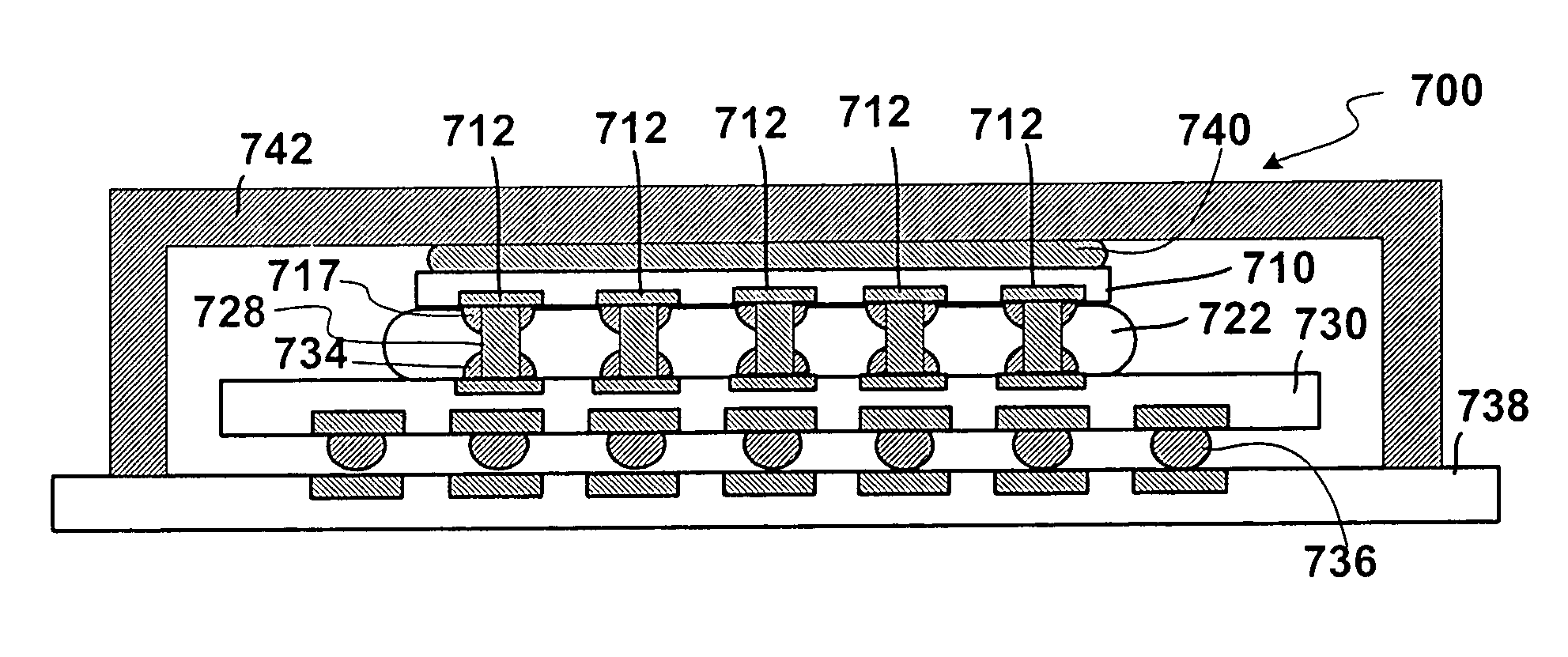
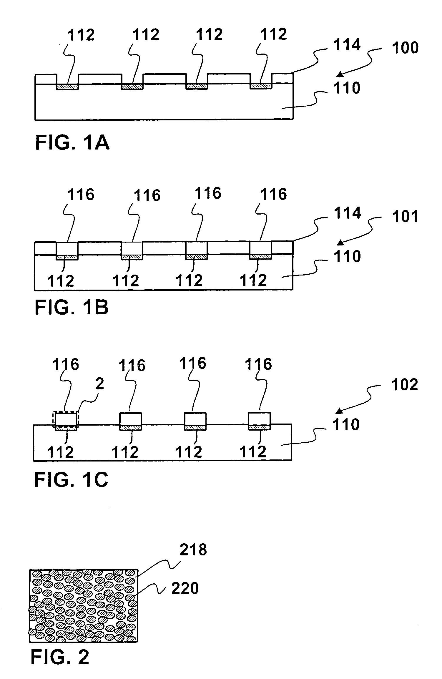
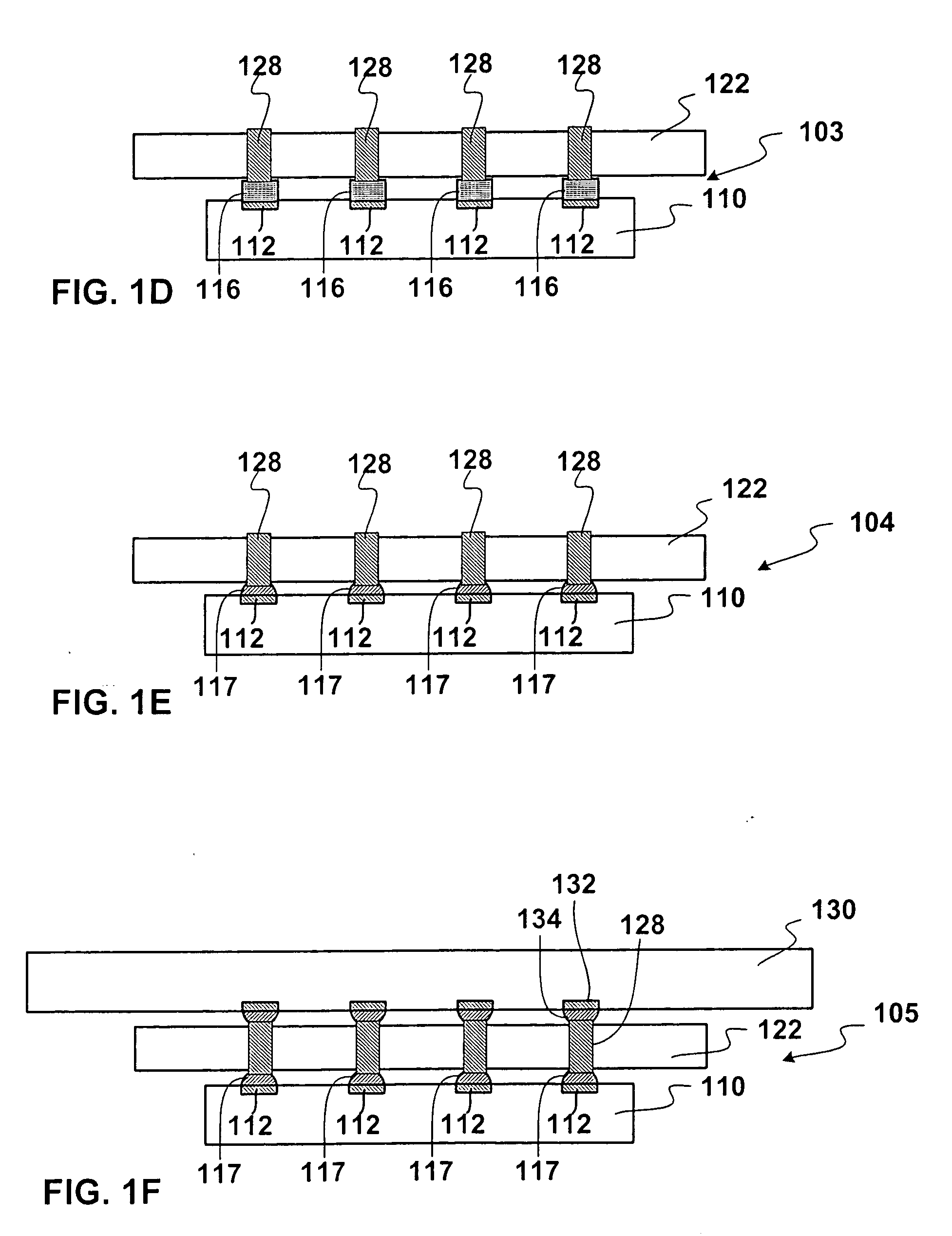
[0019] The following description includes terms, such as upper, lower, first, second, etc., that are used for descriptive purposes only and are not to be construed as limiting. The embodiments of a device or article described herein can be manufactured, used, or shipped in a number of positions and orientations. The terms “die” and “chip” generally refer to the physical object that is the basic workpiece that is transformed by various process operations into the desired integrated circuit device. A die is usually singulated from a wafer, and wafers may be made of semiconducting, non-semiconducting, or combinations of semiconducting and non-semiconducting materials. A board is typically a resin-impregnated fiberglass structure that acts as a mounting substrate for the die.

[0020] An embodiment relates to a wire interconnect that is embedded in a nanosolder. The nanosolder is derived from a solder paste that includes a metal particle having a diameter in a range from about 2 nanometer...


PUM


Abstract

A nano-sized metal particle composite includes a first metal that has a particle size of about 50 nanometer or smaller. A wire interconnect is in contact with a reflowed nanosolder and has the same metal or alloy composition as the reflowed nanosolder. A microelectronic package is also disclosed that uses the reflowed nanosolder composition. A method of assembling a microelectronic package includes preparing a wire interconnect template. A computing system includes a nanosolder composition coupled to a wire interconnect.

Description

TECHNICAL FIELD [0001] Disclosed embodiments relate to nano-sized solder paste compositions for use in microelectronic device packaging. BACKGROUND INFORMATION [0002] An integrated circuit (IC) die is often fabricated into a processor for various tasks. IC operation invariably leads to heat generation and thermal expansion stresses in a die package. High melting point solder, although they withstand the high operating temperatures caused by the densely packed circuitry in a die, requires high processing temperature, which can cause high thermal-mechanical stress due to coefficient of thermal expansion (CTE) mismatch between semiconductive die and organic substrate. But for low melting solder, the electro-migration is much more easily to happen. Additionally, corrosion can occur between the two disparate metals of the solder bump and the bond pad.BRIEF DESCRIPTION OF THE DRAWINGS [0003] In order to understand the manner in which embodiments are obtained, a more particular description...

Claims


Application Information

Patent Timeline
IPC IPC(8): H01L23/02
CPCH01L21/4846H01L21/486H01L24/13H01L2924/014H01L2924/01047H01L2924/01019H01L2924/01006H01L2924/01005H01L2224/73204H01L2224/32225H01L2224/16225H01L2924/16152H01L2924/15311H01L2924/1433H01L23/36H01L23/49816H01L23/49827H01L24/10H01L2224/13099H01L2224/73253H01L2924/01015H01L2924/01029H01L2924/01033H01L2924/01078H01L2924/01079H01L2924/01082H01L2924/12044H01L2924/14H01L2924/00H01L2224/13H01L2224/05571H01L2224/05573H01L2224/05647H01L2224/16235H01L2224/13499H01L2224/1152H01L24/05H01L24/11H01L24/16H01L24/32H01L24/73H01L24/81H01L24/83H01L24/92H01L2224/0401H01L2224/11849H01L2224/13294H01L2224/16227H01L2224/81191H01L2224/81815H01L2224/83191H01L2224/13311H01L2224/13316H01L2224/13444H01L2224/13411H01L2224/05554H01L2224/1141H01L2224/11436H01L2224/1147H01L2224/131H01L2224/13111H01L2224/13144H01L2224/133H01L2224/13339H01L2224/13344H01L2224/13347H01L2224/27436H01L2224/8385H01L2224/9211H01L2224/11848H01L2224/13447H01L2224/13416H01L2224/13439H01L2924/00014H01L2924/00012H01L2924/0105H01L2224/11H01L2224/27H01L2224/81H01L2224/83H01L21/48H01L23/48
Inventor HUA, FAY
Owner INTEL CORP
Why Eureka
Try Eureka