Liquid crystal display device and method for manufacturing the same

a liquid crystal display and active matrix technology, applied in non-linear optics, instruments, optics, etc., can solve problems such as disturbance of the electric field applied to the liquid crystal from an electrode, and achieve the effect of preventing the decrease of the aperture ratio

Inactive Publication Date: 2007-01-04
SEMICON ENERGY LAB CO LTD
View PDF19 Cites 65 Cited by
  • Summary
  • Abstract
  • Description
  • Claims
  • Application Information

AI Technical Summary

Benefits of technology

[0030] The coloring film of the active matrix substrate is provided at the opposite side from a liquid crystal with respect to the pixel electrode; therefore, the coloring film can be formed in the active matrix substrate without affecting an application of an electric field with respect to the liquid crystal from both of the electrodes.
[0031] In the present invention, in a case where a TFT which is formed in an active matrix substrate is a bottom gate TFT having an active layer formed from an amorphous semiconductor, a semiamorphous semiconductor, or a polycrystalline semiconductor and also a case where a light source is provided at a counter substrate side, when a light-shielding body is provided at a position which is overlapped with the active layer, a leak current can be prevented from being generated between a source region and a drain region in a case of driving the TFT as well as the above effect. Further, in a case of providing the light-shielding body, by forming the bottom gate TFT as a channel stop (protection) type, the light-shielding body can be provided without increasing the number of processes.
[0032] In addition, in the present invention, in a case where a pixel electrode (individual electrode) and a counter electrode (common electrode) are formed in a pixel portion of an active matrix substrate, by forming one or both of the electrodes by using a transparent conductive film, an aperture ratio can be prevented from decreasing as well as the above effect. Note that a top gate TFT may be used as the TFT of the present invention, although the bottom gate TFT is shown.

Problems solved by technology

However, when a structure is used, in which a coloring film is formed over a pixel electrode like the liquid crystal display device of the above-described document, a structure in which a dielectric is interposed between the pixel electrode and a liquid crystal is obtained; therefore, a problem occurs, in which an electric field which is applied to the liquid crystal from an electrode is disturbed.

Method used


Image

  • Liquid crystal display device and method for manufacturing the same
  • Liquid crystal display device and method for manufacturing the same
  • Liquid crystal display device and method for manufacturing the same

Examples


embodiment mode 1

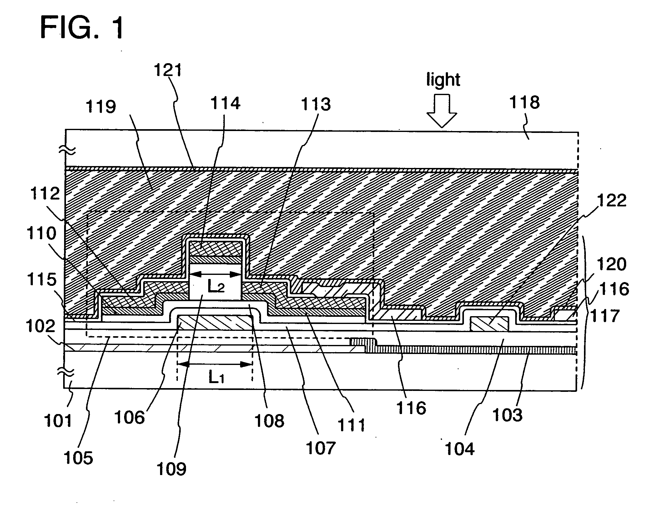
[0047] In Embodiment Mode 1, among liquid crystal panels that can be used for a liquid crystal display device of the present invention, a liquid crystal display panel which is driven by an In-Plain Switching system (such as an IPS mode or an FFS mode), in which a pixel electrode (individual electrode) and a counter electrode (common electrode) are formed in an active matrix substrate, will be explained with reference to FIG. 1.

[0048] In FIG. 1, a light-shielding film 102 is formed over a substrate 101, and a coloring film 103 is formed so as to be overlapped with part of the light-shielding film 102.

[0049] A glass substrate, a quartz substrate, a substrate formed from an insulating substance such as ceramic such as alumina, a plastic substrate, a silicon wafer, a metal plate, or the like can be used for the substrate 101.

[0050] The light-shielding film 102 is patterned to be formed so as to cover all of the periphery of each pixel in a pixel portion or part thereof. As a material...

embodiment mode 2

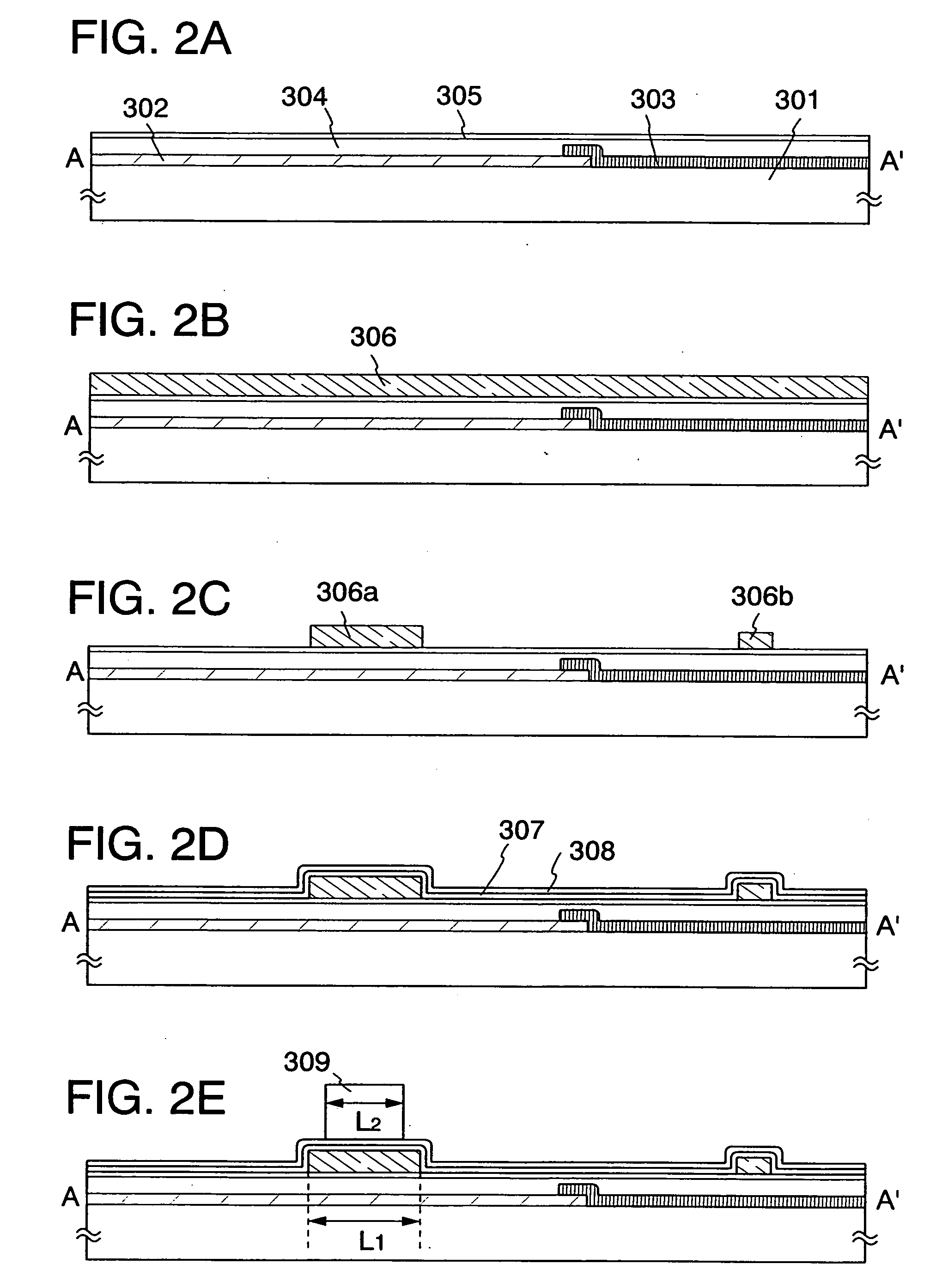
[0069] In Embodiment Mode 2, a method for manufacturing an active matrix substrate included in the liquid crystal display panel explained in Embodiment Mode 1 will be explained with reference to FIGS. 2A to 2E, FIGS. 3A to 3D, and FIG. 4. Note that FIG. 4 is a plan view of an active matrix substrate, and FIGS. 2A to 2E and FIGS. 3A to 3D are cross-sectional views taken along line A-A′ in FIG. 4. Also, same reference numerals are used in FIGS. 2A to 2E, FIGS. 3A to 3D, and FIG. 4.

[0070] First, as shown in FIG. 2A, a light-shielding film 302 is formed over a substrate 301.

[0071] As the substrate 301, a glass substrate, a quartz substrate, a substrate made of an insulating substance such as ceramic such as alumina, a plastic substrate, a silicon wafer, a metal plate, or the like can be used. In addition, a large-sized substrate having a size of 320×400 mm, 370×470 mm, 550×650 mm, 600×720 mm, 680×880 mm, 1000×1200 mm, 1100×1250 mm, or 1150×1300 mm can be used.

[0072] Note that as a re...

embodiment mode 3

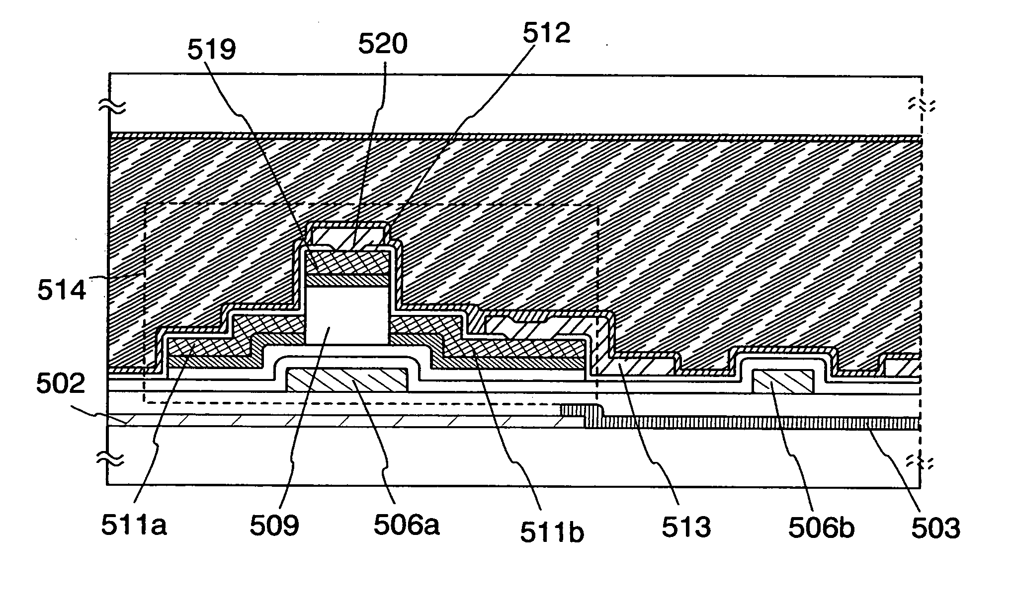
[0094] In Embodiment Mode 3, a liquid crystal display panel in which part of the structure of Embodiment Mode 1 is improved will be explained. Note that, in a liquid crystal display panel shown in FIG. 5, as for a case of denoting the similar name or the like to that in FIG. 1 explained in Embodiment Mode 1, the liquid crystal display panel can be formed by the similar material in the similar manner, and the description in Embodiment Mode 1 is referred for the detail.

[0095] A light-shielding body 519 of FIG. 5 is formed of a second conductive film which forms a source electrode 511a and a drain electrode 511b in the same manner as Embodiment Mode 1; therefore, the light-shielding body 519 is formed from a conductive material. Therefore, in a case where an insulator 509 is not formed having enough thickness, there is a case where the light-shielding body 519 becomes parasitic capacitance of a TFT 514. Thus, in Embodiment Mode 3, in order to prevent the light-shielding body 519 from ...


PUM

PropertyMeasurementUnit
temperatureaaaaaaaaaa
thicknessaaaaaaaaaa
thicknessaaaaaaaaaa

Abstract

In the present invention, it is an object to provide a liquid crystal display device in which a precise position alignment in attaching an active matrix substrate and a counter substrate is unnecessary and also does not affect an application of an electric field to a liquid crystal from an electrode, and a manufacturing method thereof. According to one feature of the present invention, the liquid crystal display device is formed using an active matrix substrate in which a driver circuit including a plurality of TFTs, a wiring, and the like, a pixel portion including a plurality of TFTs, a wiring, a pixel electrode, and the like are formed over a substrate provided with a light-shielding film and a coloring film, and the liquid crystal display device has a structure in which a liquid crystal is injected between the active matrix substrate and the counter substrate.

Description

BACKGROUND OF THE INVENTION [0001] 1. Field of the Invention [0002] The present invention relates to an active matrix liquid crystal display device and a method for manufacturing the same. [0003] 2. Description of the Related Art [0004] An active matrix liquid crystal display device using an active element such as a thin film transistor (TFT) has been conventionally known. An active matrix liquid crystal display device can increase pixel density, is small and lightweight, and also consumes low power; therefore, a product such as a monitor of a personal computer, a liquid crystal TV, or a monitor of a car navigation system has been developed as one of flat panel displays which is a substitute for CRT. [0005] As for a liquid crystal display device, a substrate (active matrix substrate) over which a driver circuit constituted by a plurality of TFTs and wirings (such as a source signal line driver circuit or a gate signal line driver circuit), a pixel portion, and the like constituted b...

Claims


Application Information

Patent Timeline
Patent Type & Authority Applications(United States)
IPC IPC(8): G02F1/136
CPCG02F1/133345G02F2001/136222G02F1/136209G02F1/136222G02F1/136
Inventor FUJIKAWA, SAISHIHOSOYA, KUNIO
Owner SEMICON ENERGY LAB CO LTD
Why Eureka
Try Eureka