Method for the preparation of group ib-iiia-via quaternary or higher alloy semiconductor films

a technology of quaternary or higher alloy semiconductor films and semiconductor films, which is applied in the direction of polycrystalline material growth, final product manufacturing, gel state, etc., can solve the problems of increasing the cost of production process, limiting the vsub>oc/sub> of the device, and negatively affecting the performance of the devi

Inactive Publication Date: 2007-01-04
JOHANNESBURG UNIV OF
View PDF2 Cites 34 Cited by
  • Summary
  • Abstract
  • Description
  • Claims
  • Application Information

AI Technical Summary

Problems solved by technology

The effect of a segregated or graded film structure with most of the gallium residing at the back of the film, is that the absorber film exhibits a low band gap value in the active region of the photovoltaic cell, which ultimately limits the Voc of the device.
In addition, in the case of extreme grading, lattice mismatches within the graded absorber films introduce electrically active structural defects, which negatively impact on the device performance.
The disadvantages of the above post-sulfurisation step, which is already applied on an industrial scale, are:
(iii) high temperatures and long reaction times of between 90 to 120 minutes are required to achieve significant degrees of S incorporation, which ultimately increases the costs of the production process; and
(iv) the resulting alloys are heterogeneous, which prohibit effective control over the lattice parameters and band gap values.
In addition, the carrying out of the post-annealing step in an inert atmosphere resulted in substantial losses of Se from the film, which necessitated a second annealing step in H2Se / Ar.
The additional post-annealing steps in an inert atmosphere as well as H2Se / Ar not only compromise the reproducibility of the process, but also make it commercially unviable.

Method used


Image

  • Method for the preparation of group ib-iiia-via quaternary or higher alloy semiconductor films
  • Method for the preparation of group ib-iiia-via quaternary or higher alloy semiconductor films
  • Method for the preparation of group ib-iiia-via quaternary or higher alloy semiconductor films

Examples


example 1

Experimental Procedure for the Production of a Group IB-IIIA-VIA Pentenary Alloy

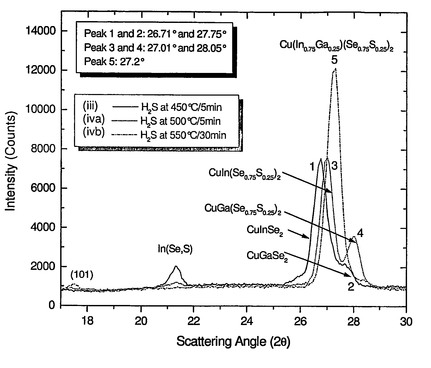
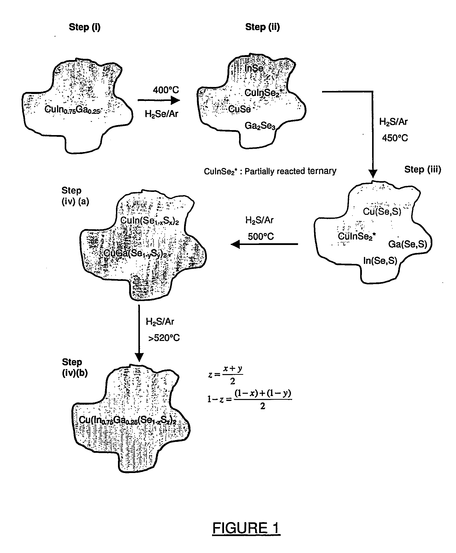
[0191]FIG. 1 is a schematic representation of the method according to the invention for the production of a group IB-IIIA-VIA pentenary alloy semiconductor film.

Step i

[0192] Step (i) was followed as set out under the general experimental procedure. More particularly, the deposition of the Mo layer was followed, without breaking vacuum, by the co-sputtering of Cu0.75Ga0.25 and In at a working pressure of 0.3 Pa. The co-sputtering of the metals, Cu, In and Ga, was also carried out without intentional substrate heating and the substrate was rotated during co-sputtering in order to enhance the mixing of the Cu—Ga—In alloy. The total thickness of the Cu—In—Ga alloys was 0.6 μm and the Cu / (In+Ga) and Ga / (Ga+In) atomic ratios were maintained at 0.9 and 0.25 respectively.

Step ii

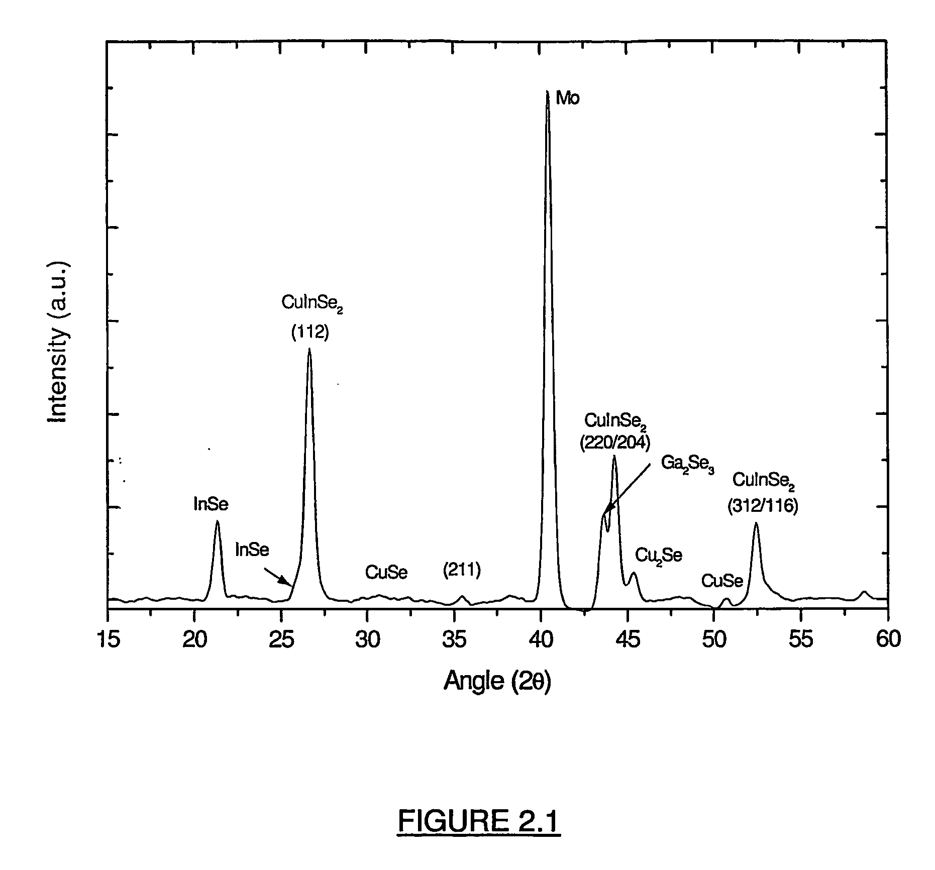
[0193] The substrate with the co-sputtered metal film of step i was placed in a horizontal quartz tube reactor (herein after refe...

example 2

Experimental Procedure for the Production of a Group IB-IIIA-VIA Quaternary Alloy

Step (i)

[0235] Step i is the same as set out under the general experimental procedure. More particularly, the deposition of the Mo layer was followed, without breaking vacuum, by the co-sputtering of Cu0.75Ga0.25 and In at a working pressure of 0.3 Pa. The co-sputtering was also carried out without intentional substrate heating and the substrate was rotated during co-sputtering in order to enhance the mixing of the Cu—Ga—In alloy. The total thickness of the Cu—In—Ga alloys was 0.6 μm and the Cu / (In+Ga)- and Ga / (Ga+In)- atomic ratios were maintained at 0.9 and 0.25 respectively.

Step ii

[0236] In this case the same method as set out in step ii of experiment 1 above was followed, however the reaction temperature was kept at 400° C. so as to form a first film comprising a stable mixture of binary alloys and CuInSe2 only.

[0237] It is believed by the inventor that in the case of the production of quater...

example 3

Experimental Procedure for the Production of a Group IB-IIIA-VIA Quaternary Alloy—Production of CuIn(Se1-ySy)2.

Step i

[0260] In this case, a metal film was prepared comprising only Cu and In, as opposed to the previous cases wherein Ga was also included. More specifically the metal precursors of Cu and In were co-sputtered onto a substrate using a Leybold Z650 DC Magnetron Sputtering System. The system accommodates three separate targets (i.e. Mo, Cu and In), and the substrate was rotated continuously during deposition in order to promote intermixing of Cu and In. The Mo back contact (about 1 μm thick) was sputtered from a 5N purity Mo target at a working pressures between 0.3 Pa to 0.7 Pa. The Mo film was cooled in vacuum to room temperature, followed by the co-sputtering of the Cu and In layers from 5N purity Cu and In targets. The total thickness of the copper-indium alloy was around 0.6 μm, and the desired Cu / In atomic ratio between 0.85-0.9 was achieved by keeping the Cu powe...


PUM

PropertyMeasurementUnit
temperatureaaaaaaaaaa
temperaturesaaaaaaaaaa

Abstract

This invention relates to a method for producing group IB-IIA-VIA quaternary or higher alloy semiconductor films wherein the method comprises the steps of (i) providing a metal film comprising a mixture of group IB and group IIIA metals; (ii) heat treating the metal film in the presence of a source of a first group VIA element (said first group VIA element hereinafter being referred to as VIA1) under conditions to form a first film comprising a mixture of at least one binary alloy selected from the group consisting of a group IB-VIA1 alloy and a group IIIA-VIA1 alloy and at least one group IB-IIIA-VIA1 ternary alloy (iii) optionally heat treating the first film in the presence of a source of a second group VIA element (said second group VI element hereinafter being referred to as VIA2) under conditions to convert the first film into a second film comprising at least one alloy selected from the group consisting of a group IB-VIA1-VIA2 alloy and a group IIIA-VIA1-VIA2 alloy; and the at least one group IB-III-VIA1 ternary alloy of step (ii); (iv) heat treating either the first film or second film to form a group IB-IIIA-VIA quaternary or higher alloy semiconductor film.

Description

FIELD OF THE INVENTION [0001] This invention relates to a method for the preparation of a semiconductor film suitable for use in a photovoltaic / solar cell, and in particular to a group IB-IIIA-VIA quaternary or higher alloy semiconductor film. BACKGROUND TO THE INVENTION Definitions [0002] For the purposes of this specification the term “pentenary alloy” refers to an alloy having 5 different elements. So for example, Cu(In,Ga)(S,Se)2 is a group IB-IIIA-VIA pentenary alloy wherein the 5 different elements are copper (Cu), indium (In), gallium (Ga), selenium (Se) and sulfur (S). Similarly the term “quaternary alloy” refers to an alloy having 4 different elements. So for example, Cu(In,Ga)Se2 is a group IB-IIIA-VIA quaternary alloy. Likewise, a ternary alloy has three different elements and a binary alloy has two different elements. [0003] The term “homogeneous” alloy means that the different elements constituting the alloy are distributed homogeneously through the alloy such that the...

Claims


Application Information

Patent Timeline
Patent Type & Authority Applications(United States)
IPC IPC(8): H01L21/00H01L31/032H01L31/18
CPCH01L31/0322Y02E10/541H01L31/18Y02P70/50C22C9/00
Inventor ALBERTS, VIVIAN
Owner JOHANNESBURG UNIV OF
Why Eureka
Try Eureka