Semiconductor storage device

Active Publication Date: 2007-01-04
HIROSHIMA UNIVERSITY +1
View PDF12 Cites 34 Cited by
  • Summary
  • Abstract
  • Description
  • Claims
  • Application Information

AI Technical Summary

Benefits of technology

[0010] The present invention was developed in order to overcome such problems. It is therefore an object of the present invention to

Problems solved by technology

However, there is a certain physical limit to a reduction in the size of the memory cell, and the increase in the chip size decreases productivity and hinders a speed increase.
The through-electrodes are therefore utilized with low efficiency, and high-speed data transfer is d

Method used


Image

  • Semiconductor storage device
  • Semiconductor storage device
  • Semiconductor storage device

Examples


Embodiment Construction

[0037] Preferred embodiments of the present invention will now be explained in detail with reference to the drawings.

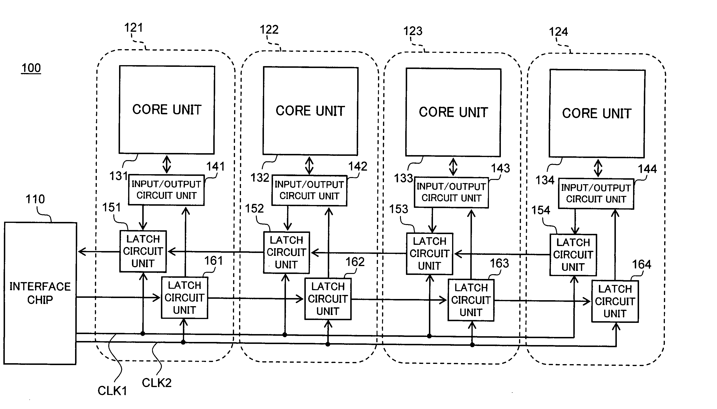
[0038]FIG. 1 is a schematic block diagram showing the circuit structure of the semiconductor storage device 100 according to a first preferred embodiment of the present invention.

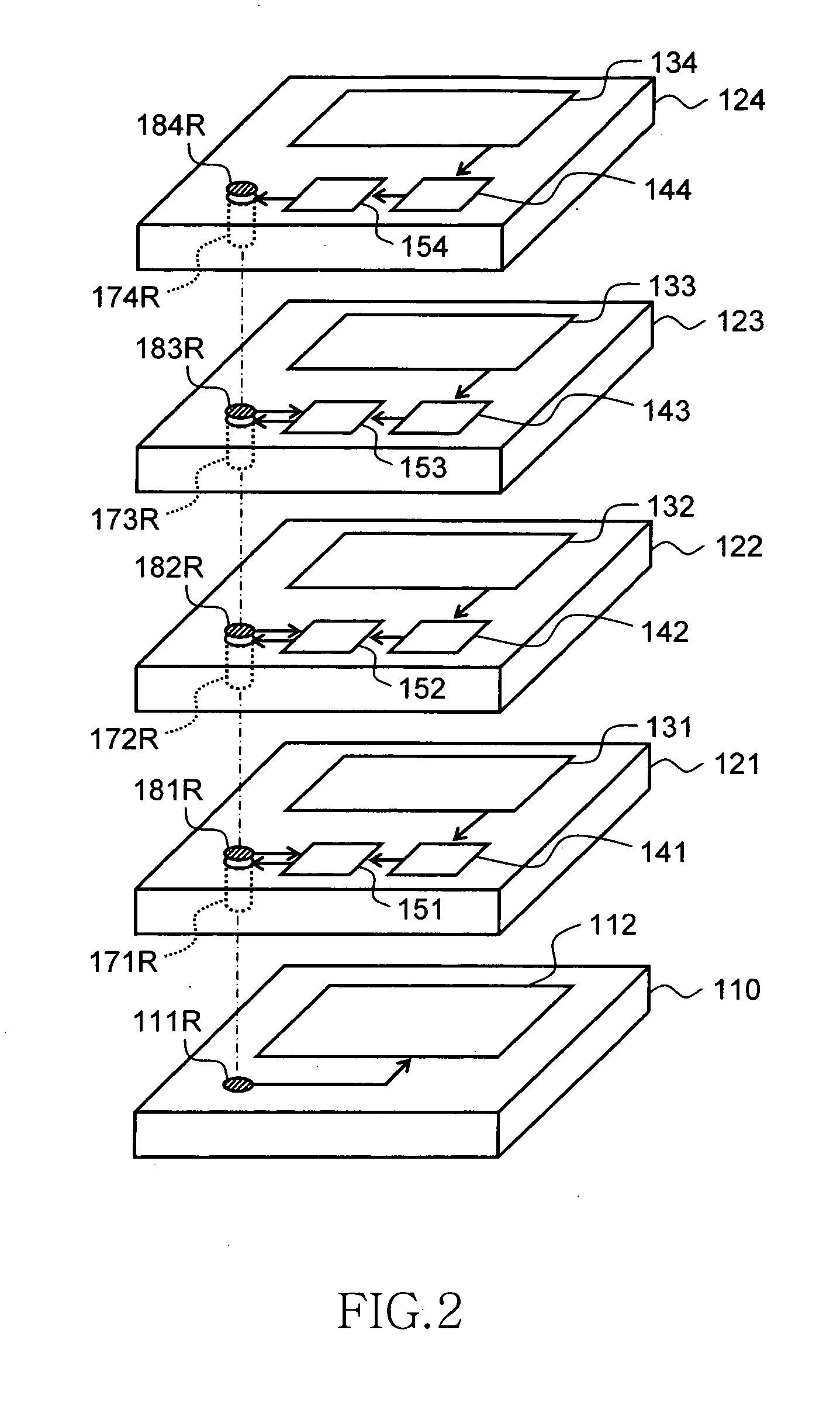
[0039] As shown in FIG. 1, the semiconductor storage device 100 according to the present embodiment includes one interface chip 110 and four core chips 121 to 124. As described hereinafter, the interface chip 110 and the core chips 121 to 124 are layered together.

[0040] The four core chips 121 to 124 are provided with core units 131 to 134 in which memory cells are formed, input / output circuit units 141 to 144, first latch circuit units 151 to 154, and second latch circuit units 161 to 164, respectively. The first latch circuit units 151 to 154 are circuits for temporarily storing the data outputted by the core units 131 to 134, and the second latch circuit units 161 to 164 are circuits fo...


PUM


Abstract

Data transfer speed is increased in a semiconductor storage device in which the core unit and the interface unit are separate chips. The device has a plurality of core chips through in which a memory cell is formed, and an interface chip in which a peripheral circuit is formed for the memory cell. The plurality of core chips through have latch circuit units through for temporarily storing data to be outputted by the memory cell, and latch circuit units through for temporarily storing data to be inputted to the memory cell, respectively, and these latch circuit units through and latch circuit units through are connected in a cascade to the interface chip. Since the plurality of latch circuit units connected in a cascade can thereby perform a pipeline operation, it becomes possible to achieve high-speed data transfer.

Description

TECHNICAL FIELD [0001] The present invention relates to a semiconductor storage device, and particularly relates to a semiconductor storage device in which separate chips are used to form a core unit in which a memory cell is formed, and to form an interface unit in which a peripheral circuit is formed for the memory cell. BACKGROUND OF THE INVENTION [0002] The storage density of a semiconductor memory device as represented by a DRAM (Dynamic Random Access Memory) is increasing in recent years, and a high speed is also required. The increase of the storage density has so far been achieved mainly by downsizing of memory cells and increase of chip sizes. However, there is a certain physical limit to a reduction in the size of the memory cell, and the increase in the chip size decreases productivity and hinders a speed increase. [0003] In order to substantially solve the above problems, there is proposed a method of using separate chips for the core section that is formed with memory c...

Claims


Application Information

Patent Timeline
IPC IPC(8): G06F12/00
CPCG11C5/02G11C7/1051G11C7/1078G11C7/1087G11C2207/107H01L23/481H01L2924/13091G11C7/1039H01L2224/16H01L2924/00H01L2224/05573H01L2224/13025H01L2924/00014H01L2224/05599
Inventor IKEDA, HIROAKISASAKI, MAMORUIWATA, ATSUSHI
Owner HIROSHIMA UNIVERSITY
Why Eureka
Try Eureka