Pixel array strcuture

Inactive Publication Date: 2007-01-11
UNITED MICROELECTRONICS CORP
View PDF3 Cites 3 Cited by
  • Summary
  • Abstract
  • Description
  • Claims
  • Application Information

AI Technical Summary

Benefits of technology

[0019] In the present invention, the titanium metal layer serves as the upmost top metal layer of the top-metal-layer structure of the CMOS, and the upmost top metal layer serves as the bottom electrode of the organic light emitting diode. Accordingly, the decay of the organic light emitting diode can be efficiently delayed, and the life time of the OLED display can be enhanced. In addition, the CMOS of the substrate controls the illumination of the organic light emitti

Problems solved by technology

Accordingly, how to extend the life time of the light emitting material is the key issue in enhancing the life time of the OLED display.
The light emitting material is likely to penetrate into the top metal laye

Method used


Image

  • Pixel array strcuture
  • Pixel array strcuture
  • Pixel array strcuture

Examples


Example

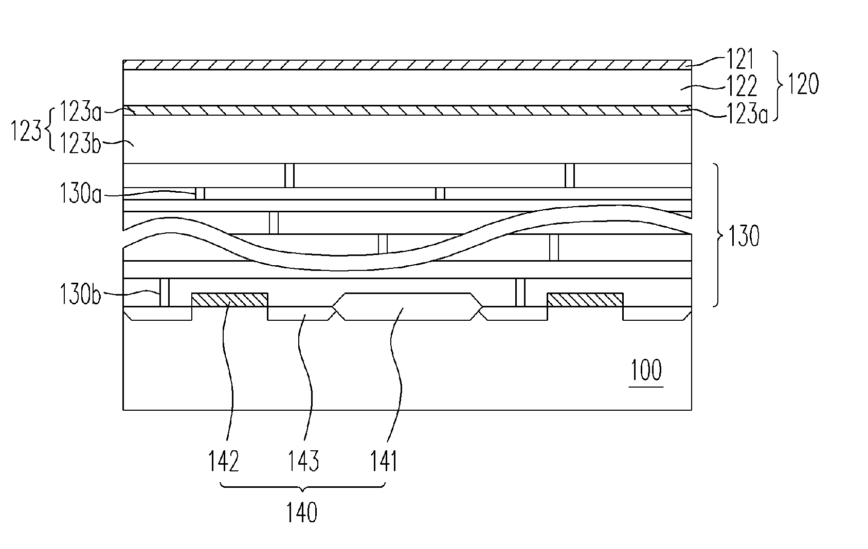
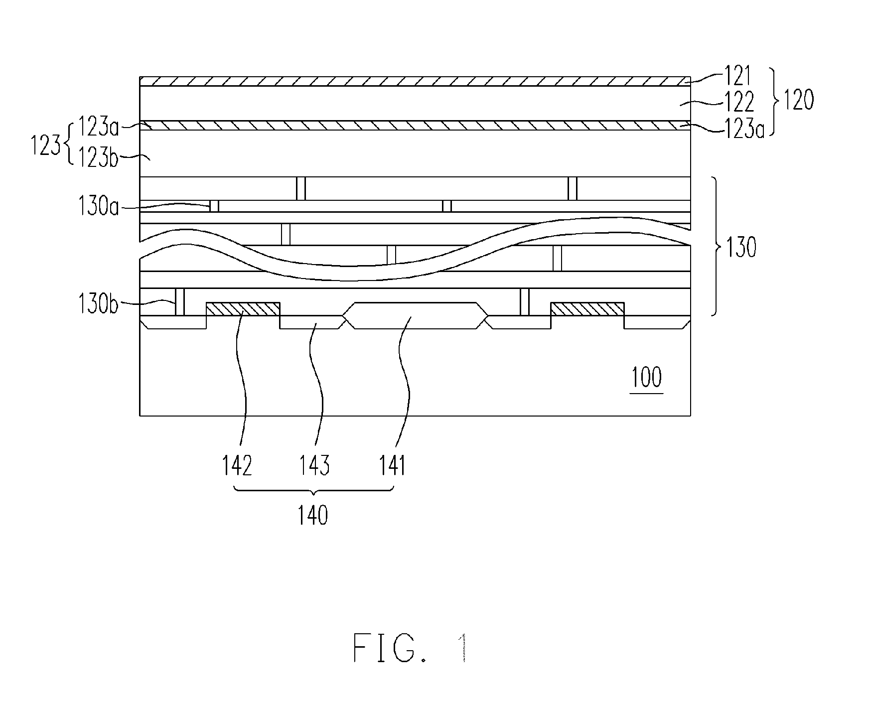
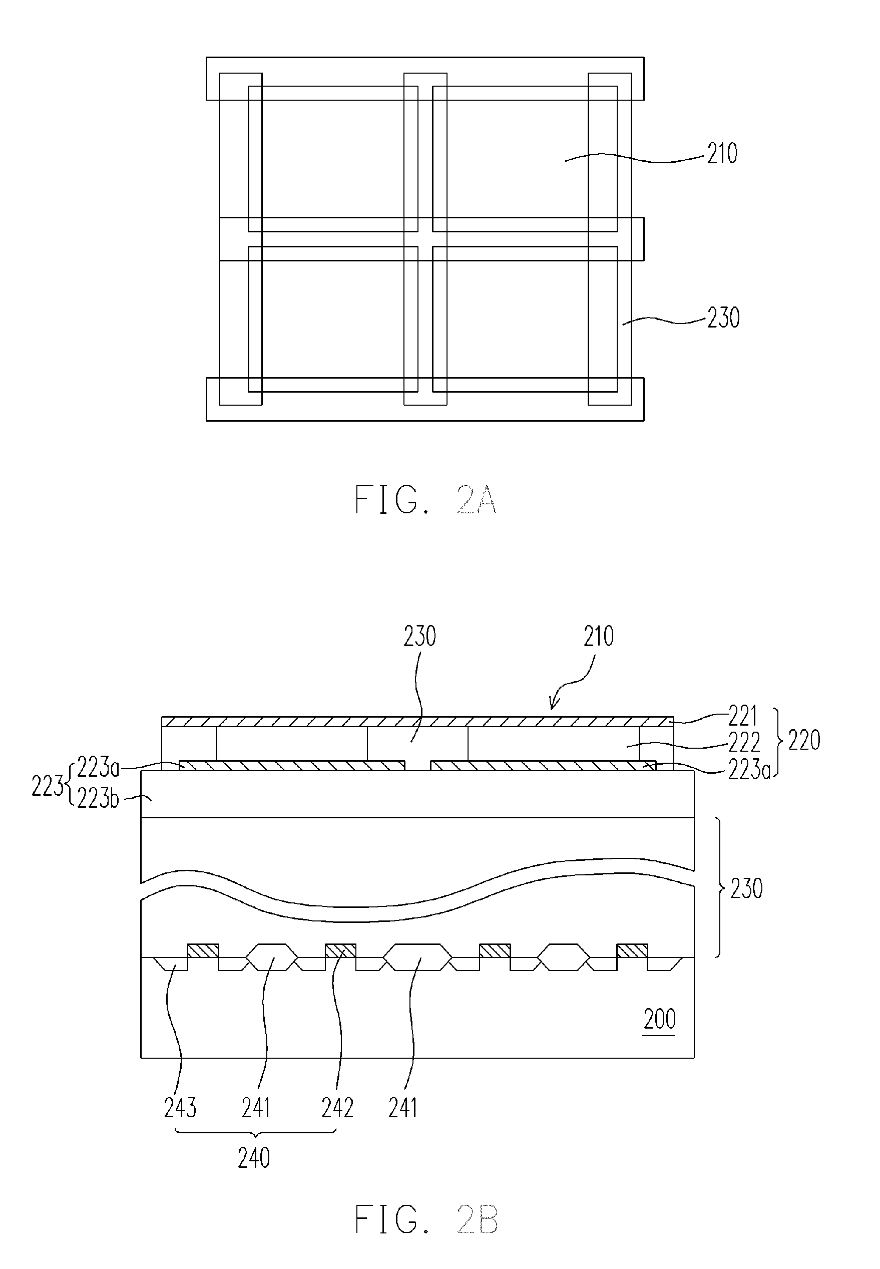
[0028]FIG. 1 is a cross sectional view of a pixel structure according to a preferred embodiment of the present invention. Referring to FIG. 1, according to the pixel structure of the preferred embodiment of the present invention, the structure comprises an organic light emitting diode (OLED) 120, and a complementary metal-oxide-semiconductor (CMOS)

[0029] 140. Wherein, the OLED 120 comprises a transparent electrode 121, a bottom electrode 123a, and a light emitting material 122 between the transparent electrode 121 and the bottom electrode 123a. The material of the transparent electrode 121 can be, for example, indium-zinc oxide, or indium-tin oxide. The light emitting material 122 can be, for example, an organic light emitting material, or a polymer light emitting material. The CMOS 140 comprises a field oxide layer 141, a gate 142, and source / drain regions 143 adjacent to two sides of the gate 142. Additionally, the CMOS 140 is disposed in a substrate 100. The substrate 100 can be...


PUM


Abstract

A pixel array structure is provided. The pixel array structure comprises a plurality of pixel units and a plurality of dielectric walls. Each dielectric wall is disposed between two neighboring pixel units, wherein each pixel unit comprises at least one organic light emitting diode and a complementary metal-oxide-semiconductor (CMOS). The organic light emitting diode comprises a transparent electrode, a bottom electrode, and a light emitting material between the transparent electrode and the bottom electrode. The CMOS is disposed in a substrate. The substrate comprises a top-metal-layer structure located thereon and the top-metal-layer structure comprises an upmost top metal layer. Further, the bottom electrode of the CMOS is the upmost top metal layer of the top-metal-layer structure and the upmost top metal layer is a titanium metal layer.

Description

BACKGROUND OF THE INVENTION [0001] 1. Field of the Invention [0002] The present invention relates to a display device structure, and more particularly to a pixel structure. [0003] 2. Description of Related Art [0004] In order to accord with diversified information equipment, flat panel displays (FPDs) have become essentially required apparatuses. To meet the future trend of displays being slim and power-saving, flat panel displays have gradually replaced cathode ray tube (CRT) displays. At present, applications of FPD technology can be categorized as follows: plasma displays, liquid crystal displays, electroluminescent displays, light emitting diode (LED) displays, vacuum fluorescent displays, field emission displays, electrochromic displays, and organic light emitting diode (OLED) displays. [0005] An OLED display comprises the following advantages: (1) no restriction of view angles; (2) low manufacturing cost; (3) high responsive speed (hundreds' times faster than that of a liquid ...

Claims


Application Information

Patent Timeline
IPC IPC(8): H01L29/08
CPCH01L27/3244H01L27/3246H01L2251/558H01L2251/5315H01L51/5221H10K59/122H10K59/12H10K50/82H10K2102/3026H10K2102/351
Inventor WU, YI-TYNGLUNG, TSUAN-LUNCHENG, CHIH-HUNGPAI, KUAN-TE
Owner UNITED MICROELECTRONICS CORP
Why Eureka
Try Eureka