Semiconductor device

a technology of semiconductors and devices, applied in the direction of semiconductor devices, electrical equipment, transistors, etc., can solve the problems of high insulation breakdown voltage, low on-resistance, and fast switching ra

Inactive Publication Date: 2007-01-11
KK TOSHIBA
View PDF20 Cites 43 Cited by
  • Summary
  • Abstract
  • Description
  • Claims
  • Application Information

AI Technical Summary

Benefits of technology

[0009] According to an aspect of the invention, there is provided a semiconductor device comprising: a first semiconductor layer of silicon carbide of a first conductivity type; a second semiconductor layer of silicon carbide of a second conductivity type selectively provided on the first semiconductor layer; a main electrode layer of silicon carbide of the first conductivity type selectively provided on the second semiconductor layer; a gate insulating film provided on the second semiconductor layer; a gate electrode formed on the gate insulating film; and a third semiconductor layer of the first conductivity type intervening a current path which is formed between the main electrode layer and the first semiconductor layer when an ON voltage is applied to the gate electrode, the third semiconductor layer being selectively provided on the first semiconductor layer and being adjacent to the second semiconductor layer, and a doping density of the third semiconductor layer being higher than a doping density of the first semiconductor layer.

Problems solved by technology

Such semiconductor devices for switching applications particularly require a high insulation breakdown voltage, low on-resistance, and fast switching rate.
In such a structure, a low on-resistance can be achieved, but the gate threshold voltage is as low as 1 to 2 volts, which is unsuitable for power semiconductor devices.
That is, an extremely low gate threshold voltage undesirably causes the MOSFET to malfunction due to noise applied to the gate electrode.

Method used


Image

  • Semiconductor device
  • Semiconductor device
  • Semiconductor device

Examples


Embodiment Construction

[0030] The embodiment of the invention will now be described with reference to the drawings.

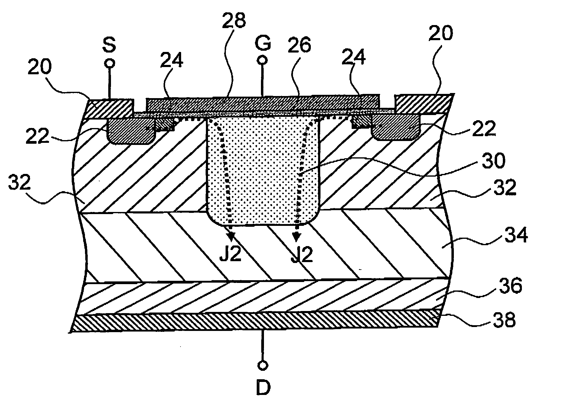
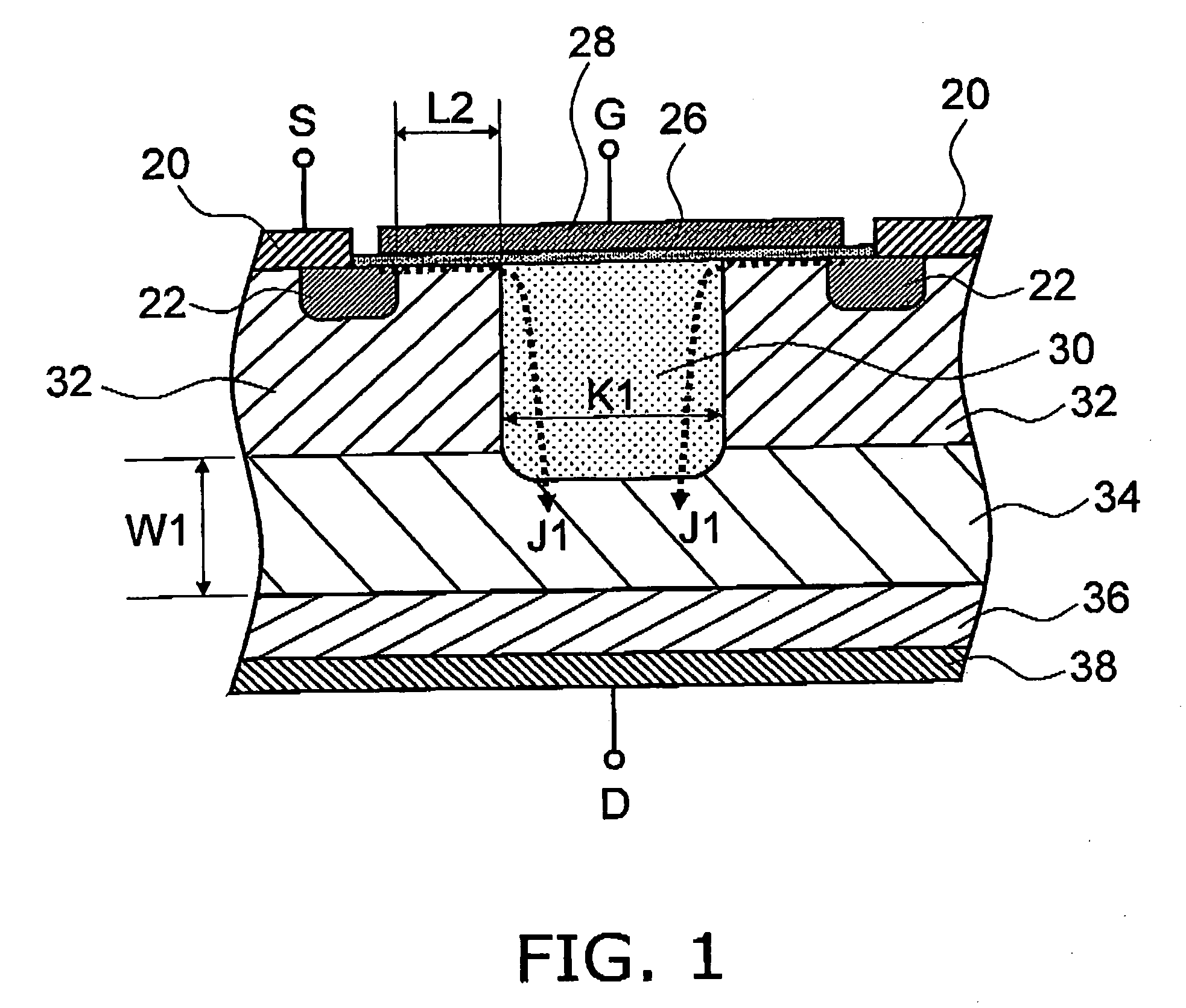
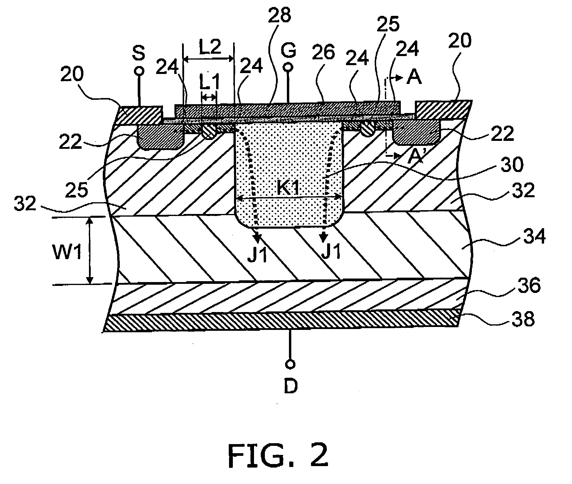
[0031]FIG. 1 is a schematic cross section of a semiconductor device according to a first example of the invention. More specifically, this figure shows a schematic cross-sectional structure of a planar MOSFET.

[0032] On an n+-type drain layer (substrate) 36 of silicon carbide (SIC) are formed an n−-type drift layer 34 and a p-type body layer 32, each made of silicon carbide. Here, when the device is illustratively designed to have a breakdown voltage of 1200 volts, the thickness W1 of the n−-type drift layer 34 is about 10 micrometers, and the thickness of the p-type body layer 32 is about 1 micrometer. An n+-type source layer (main electrode layer) 22 of the MOSFET is provided partially on top of the p-type body layer 32. An n-type layer 30 constituting the current path to the drain provided on the n+-type drain layer (substrate) 36 side is provided so as to be connected to the n−-type drif...


PUM


Abstract

A semiconductor device comprises: a first semiconductor layer of silicon carbide of a first conductivity type; a second semiconductor layer of silicon carbide of a second conductivity type selectively provided on the first semiconductor layer; a main electrode layer of silicon carbide of the first conductivity type selectively provided on the second semiconductor layer; a gate insulating film provided on the second semiconductor layer; a gate electrode formed on the gate insulating film; and a third semiconductor layer of the first conductivity type intervening a current path which is formed between the main electrode layer and the first semiconductor layer when an ON voltage is applied to the gate electrode. The third semiconductor layer is selectively provided on the first semiconductor layer and is adjacent to the second semiconductor layer. A doping density of the third semiconductor layer is higher than a doping density of the first semiconductor layer.

Description

CROSS-REFERENCE TO RELATED APPLICATIONS [0001] This application is based upon and claims the benefit of priority from the prior Japanese Patent Application No. 2005-195255, filed on Jul. 4, 2005; the entire contents of which are incorporated herein by reference. BACKGROUND OF THE INVENTION [0002] 1. Field of the Invention [0003] This invention relates to a semiconductor device, and more particularly to a semiconductor device based on silicon carbide. [0004] 2. Background Art [0005] MOS semiconductor devices based on silicon materials are widely used for power switching and high-frequency switching applications. Such semiconductor devices for switching applications particularly require a high insulation breakdown voltage, low on-resistance, and fast switching rate. As compared with silicon, silicon carbide (SiC) has about ten times higher breakdown electric field and about three times higher thermal conductivity. For this reason, silicon carbide has the great potential as a material ...

Claims


Application Information

Patent Timeline
Patent Type & Authority Applications(United States)
IPC IPC(8): H01L31/0312
CPCH01L21/26586H01L29/7828H01L29/0696H01L29/086H01L29/0869H01L29/0878H01L29/1033H01L29/1045H01L29/105H01L29/1095H01L29/1608H01L29/41766H01L29/42368H01L29/66068H01L29/7397H01L29/7802H01L29/7813H01L29/0619
Inventor OGURA, TSUNEOOMURA, ICHIRO
Owner KK TOSHIBA
Why Eureka
Try Eureka