
Method of improving magnetron sputtering of large-area substrates using a removable anode

Inactive Publication Date: 2007-01-18
APPLIED MATERIALS INC
View PDF79 Cites 6 Cited by
  • Summary
  • Abstract
  • Description
  • Claims
  • Application Information

AI Technical Summary

Benefits of technology

[0013] Embodiments of the invention may further provide a method of enhancing the uniformity of a sputter deposition process on a substrate, comprising: providing a sputter deposition chamber that has one or more walls that form a processing region, a target, and two or more anode assemblies positioned below the target and within the processing region, wherein the two or more anode assemblies are in electrical communication with an anodic surface positioned within the processing region, and depositing a layer on a surface of a substrate positioned in the processing region by cathodically biasing the target relative to the two or more anode assemblies and the anodic surface using a power supply.
[0014] Embodiments of the invention may further provide a method of enhancing the uniformity of a sputter deposition process on a substrate, comprising: positioning an anode member in a processing region formed between a target and a processing surface of a substrate positioned on a substrate support, wherein the step of positioning the anode member comprises, positioning a first member in the processing region, wherein the first member is in electrical communication with an anodic shield, and positioning one or more second members on the first member, wherein the one or more second members are in electrical communication with the first member and are adapted to cover at least a portion of the first member to prevent sputtered material from the target depositing on the first member, and depositing a layer on the processing surface by applying a bias between the target and the anodic shield.

Problems solved by technology

However, conventional sputtering presents challenges in the formation of advanced integrated circuits on large area substrates, such as flat panel display substrates.
One issue that arises is that it is generally not feasible to create a chamber big enough to maintain the surface area ratio of the cathode (target) to anode surface area commonly used in conventional sputter processing chambers.
Trying to maintain the surface area ratio can lead to manufacturing difficulties due to the large size of the parts required to achieve the desired area ratio and processing problems related to the need to pump down such a large volume to a desired base pressure prior to processing.
The insufficient anode area problem thus manifests itself as a film thickness non-uniformity that is smaller near the center of the substrate relative to the edge.
One problem with the anode structure(s) retained, or installed, in the processing region is that over time the target material is continually deposited on the substrates during processing, thus causing the size and shape of the structures to vary with time.
The deposition of the target material on the structures also increases the probability that the material deposited thereon will crack and flake during processing, due to intrinsic or extrinsic stress formed in the films deposited on these structures.
Cracking and flaking of the deposited film can generate particles that can affect the yield of the devices formed using this process.
One issue that arises in the prior art configurations is that they require the removal of major components from the process chamber, such as the target and / or PVD chamber lid (e.g., target, magnetron, shields), to access and remove the installed additional anode structures.
This process of removing major components from the process chamber can be costly and time consuming, due to the exposure of the chamber to atmospheric contamination (e.g., water, reactive gases) which will require a significant amount of time to bakeout the PVD chamber before processing can continue.
Also, removal of the major chamber components causes the film deposited on shield components from prior PVD process steps to oxidize, or become contaminated, which can thus require their removal and replacement due to particle contamination concerns.
Also, the installation of the major components back onto the process chamber can be very time consuming, since they will require the precise alignment of the target to the installed anode surface(s) to prevent arcing and sputtering of undesirable areas of the target.

Method used


Image

  • Method of improving magnetron sputtering of large-area substrates using a removable anode
  • Method of improving magnetron sputtering of large-area substrates using a removable anode
  • Method of improving magnetron sputtering of large-area substrates using a removable anode

Examples


Embodiment Construction

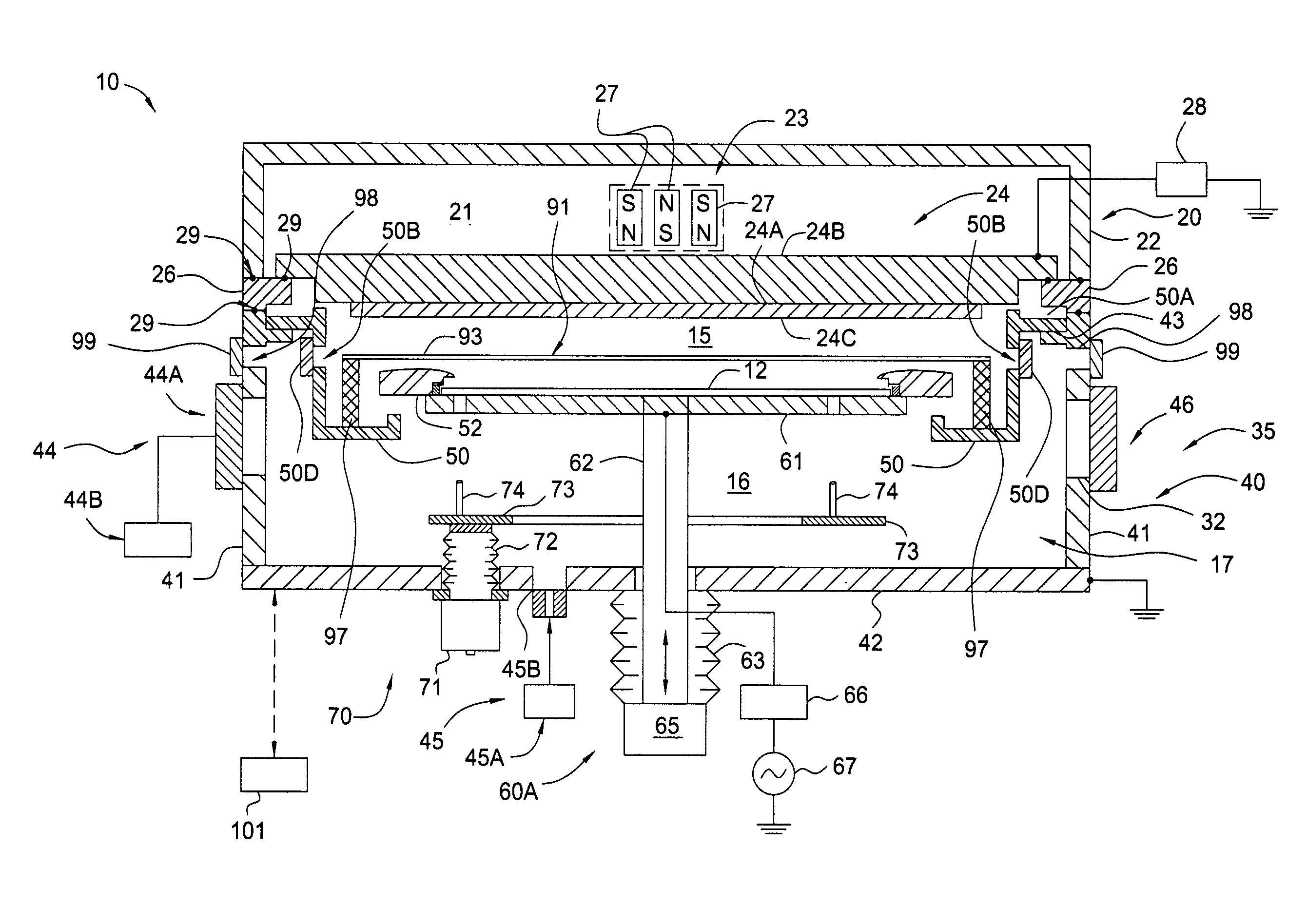
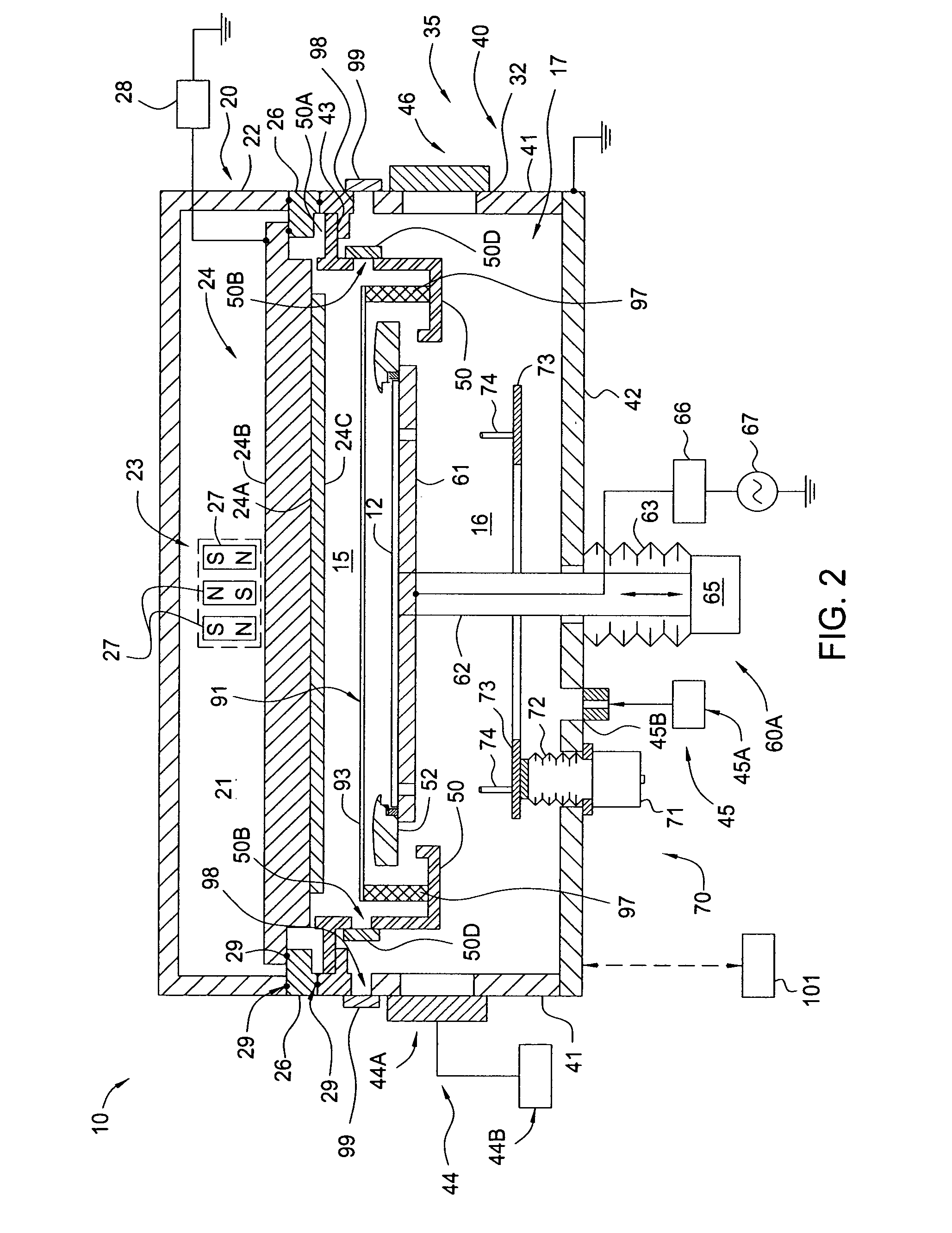
[0045] The present invention generally provides an apparatus and method for processing a surface of a substrate in a PVD chamber that has an increased anode surface area to improve the deposition uniformity. In general, aspects of the present invention can be used for flat panel display processing, semiconductor processing, solar cell processing, or any other substrate processing. The invention is illustratively described below in reference to a physical vapor deposition system, for processing large area substrates, such as a PVD system, available from AKT, a division of Applied Materials, Inc., Santa Clara, Calif. In one embodiment, the processing chamber is adapted to process substrates that have a surface area of at least about 2000 cm2. In another embodiment, the processing chamber is adapted to process substrates that have a surface area of at least about 19,500 cm2 (e.g., 1300 mm×1500 mm). However, it should be understood that the apparatus and method may have utility in other...


PUM

PropertyMeasurementUnit
Surface areaaaaaaaaaaa
Shapeaaaaaaaaaa
Electrical conductoraaaaaaaaaa

Abstract

The present invention generally provides an apparatus and method for processing a surface of a substrate in physical vapor deposition (PVD) chamber that has an increased anode surface area to improve the deposition uniformity on large area substrates. In general, aspects of the present invention can be used for flat panel display processing, semiconductor processing, solar cell processing, or any other substrate processing. In one aspect, the processing chamber contains one or more anode assemblies that are used to increase and more evenly distribute the anode surface area throughout the processing region of the processing chamber. In one aspect, the anode assembly contains a conductive member and conductive member support. In one aspect, the processing chamber is adapted to allow the conductive member to be removed from the processing chamber without removing any major components from the processing chamber.

Description

CROSS-REFERENCE TO RELATED APPLICATIONS [0001] This application claims benefit of U.S. Provisional Patent Application Ser. No. 60 / 699,428 [APPM 10196L], filed Jul. 13, 2005, which is herein incorporated by reference. This application is a continuation-in-part of co-pending U.S. patent application Ser. No. 11 / 182,034 [APPM 10196], filed Jul. 13, 2005, which is herein incorporated by reference.BACKGROUND OF THE INVENTION [0002] 1. Field of the Invention [0003] Embodiments of the present invention generally relate to substrate plasma processing apparatuses and methods that are adapted to deposit a film on a surface of a substrate. [0004] 2. Description of the Related Art [0005] Physical vapor deposition (PVD) using a magnetron is one of the principal methods of depositing metal onto a semiconductor integrated circuit to form electrical connections and other structures in an integrated circuit device. During a PVD process a target is electrically biased so that ions generated in a proce...

Claims


Application Information

Patent Timeline
IPC IPC(8): C23C14/32
CPCC23C14/35H01J37/3438H01J37/3408C23C14/564
Inventor HOSOKAWA, AKIHIROLE, HIENMINH H.INAGAWA, MAKOTOWHITE, JOHN
Owner APPLIED MATERIALS INC
Features
  • Generate Ideas
  • Intellectual Property
  • Life Sciences
  • Materials
  • Tech Scout
  • Unparalleled Data Quality
  • Higher Quality Content
  • 60% Fewer Hallucinations
Learn More