Method for driving semiconductor device having capacitive load, method and apparatus for driving load, and electronic apparatus

a semiconductor device and capacitive load technology, applied in the direction of radio frequency controlled devices, television system scanning details, television systems, etc., can solve the problems of inappropriate driving, inappropriate driving, inappropriate driving,

Inactive Publication Date: 2007-01-18
SONY CORP
View PDF6 Cites 25 Cited by
  • Summary
  • Abstract
  • Description
  • Claims
  • Application Information

AI Technical Summary

Benefits of technology

[0032] It is thus desirable to provide a mechanism that permits high-speed reading of signal with noise generation due to interference between

Problems solved by technology

However, constant current driving, if merely used, is subject to variations in the manufacture of load capacitance and variations in the manufacture of a driving device, and environmental variations, and appropriate driving may not be performed.
If phase relationship is shifted due to variations in the manufacture of load capacitance and variations in the manufacture of a driving device, appropriate driving may not be performed.
The problem is also possible if an inductive react

Method used


Image

  • Method for driving semiconductor device having capacitive load, method and apparatus for driving load, and electronic apparatus
  • Method for driving semiconductor device having capacitive load, method and apparatus for driving load, and electronic apparatus
  • Method for driving semiconductor device having capacitive load, method and apparatus for driving load, and electronic apparatus

Examples


first embodiment (

Noise Control Technique)

[0166]FIGS. 6A and 6B and FIGS. 7A and 7B illustrate a noise control method of a first embodiment of the present invention. FIGS. 6A and 6B are timing diagrams illustrating driving timing for driving the CCD solid-state image pickup element 10 of FIG. 1 in accordance with the first embodiment of the present invention. FIGS. 7A and 7B are timing diagrams illustrating the driving timing of a comparative example.

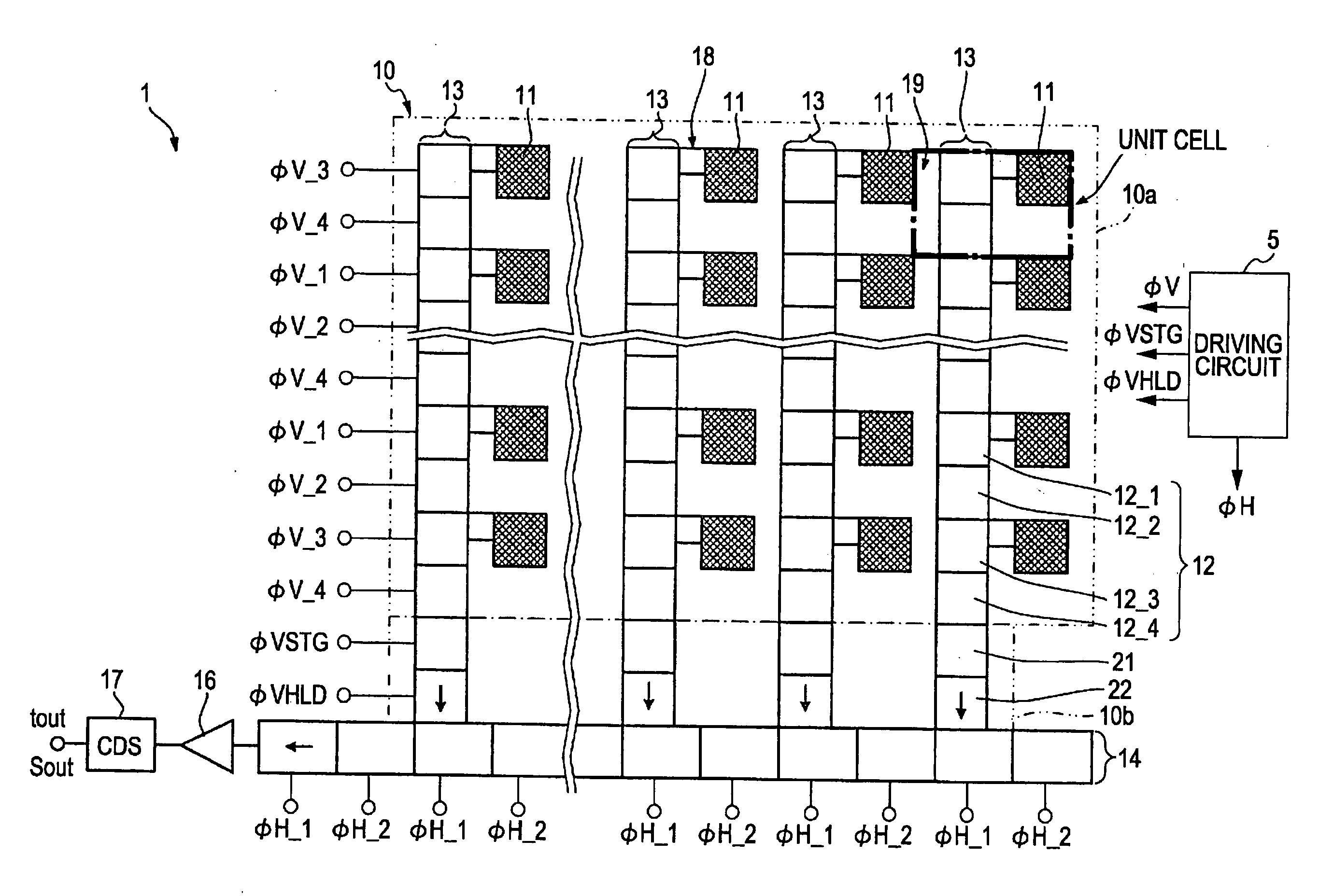
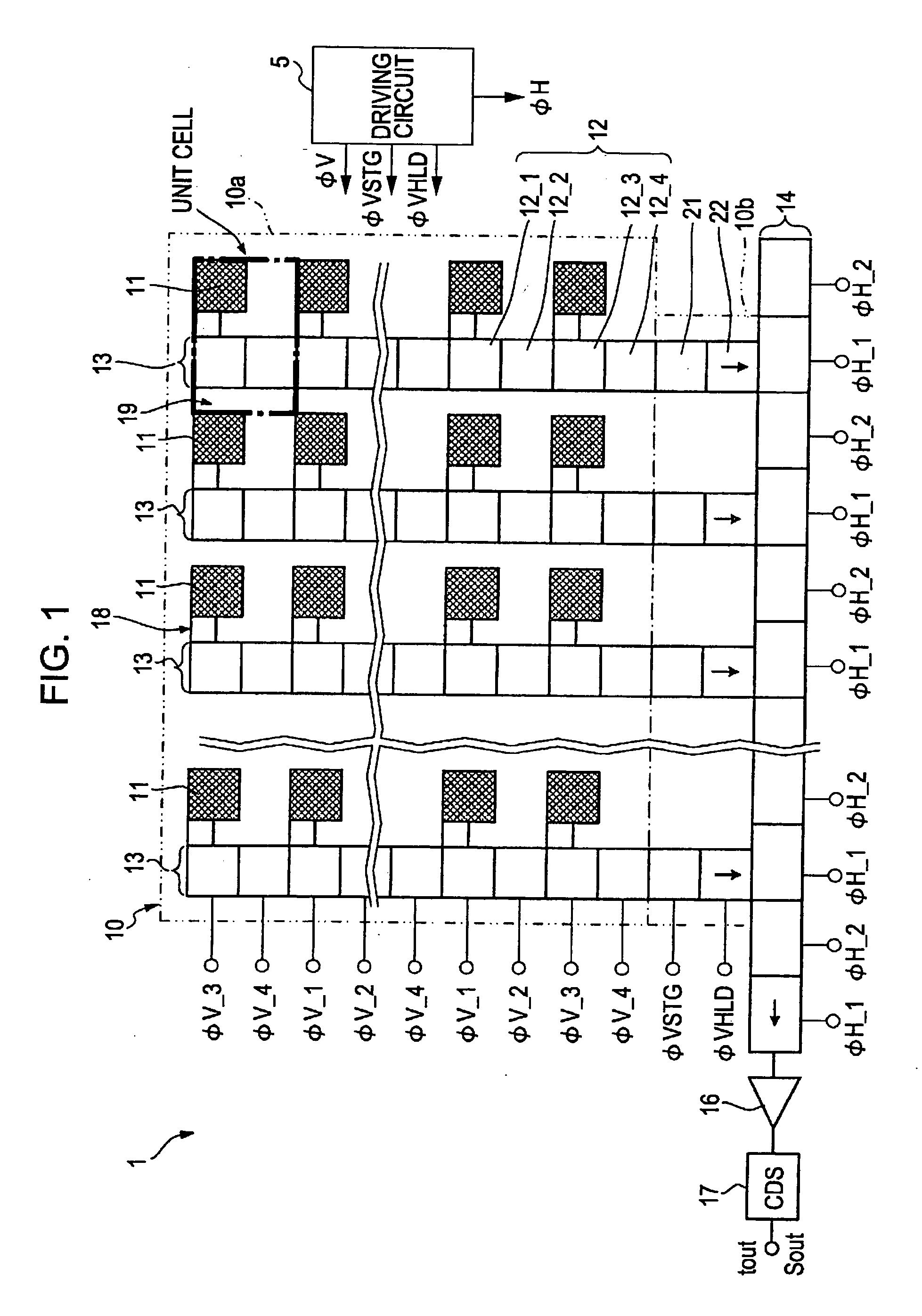
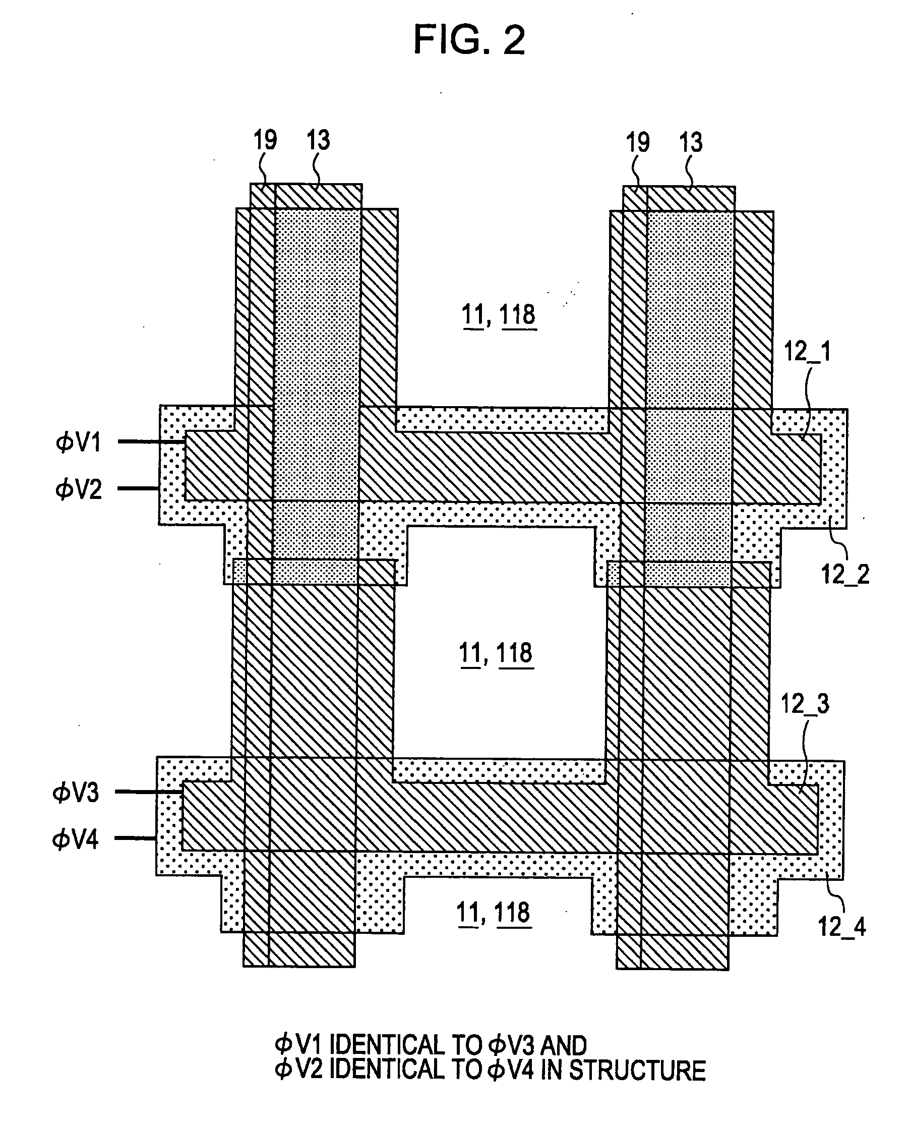
[0167] The control method of the first embodiment of the present invention is related to the four types of timing of the vertical transfer pulses ΦV supplied to the vertical transfer electrodes 12 for vertically driving the vertical transfer registers 13.

[0168] In the CCD solid-state image pickup element 10, the signal charge is received by and photoelectrically converted by the photo sensor 11 in response to the amount of light and is then stored in photo sensor 11. The signal charge of the photo sensor 11 is then read into the vertical transfer regis...

second embodiment (

Noise Control Technique)

[0227]FIG. 19 illustrates a noise control method in accordance with a second embodiment of the present invention. The noise control method of the second embodiment relates to an active control method that actively controls noise arising from cross-talk noise (coupling noise) induced on PWELL-#2b and the semiconductor substrate SUB in the CCD solid-state image pickup element.

[0228] The conventional vertical driver 40 is used as a vertical driver, and vertical transfer pulses ΦV different in phase having a sharp transient characteristic as in the known art are used.

[0229] As shown in the sectional view of FIG. 3C, the VSUB terminal 130 on the semiconductor substrate NSUB is supplied with the DC bias Vbias, and the PWELL ground terminal 132 of the PWELL-#2a on the side of the output amplifier 16 is connected to the ground GND. Using these terminals, a noise correction signal is supplied from the outside to cancel the coupling noise.

[0230] As shown in FIG. 19,...

third embodiment (

Noise Control Technique)

[0237]FIGS. 20A-20E illustrate a noise control method of a third embodiment of the present invention. The noise control method of the third embodiment relates to a noise control circuit such as a low-pass filter arranged between a vertical driver and a CCD solid-state image pickup element. The third embodiment is largely different from the known art because it is considered important in the known art that the driving signal from the vertical driver should be transferred to a vertical transfer electrode in a form as close as possible to the original shape thereof.

[0238] If the vertical transfer pulse ΦV supplied from the vertical driver 40 is supplied to the vertical transfer electrode via the noise control circuit, the cross-talk noise due to spike noise can be reduced even if unpredicted spike noise is generated in the output of the vertical driver.

[0239] The known vertical driver 40 is herein used as a vertical driver, and vertical transfer pulses ΦV diff...


PUM


Abstract

When a signal is read from a CCD solid-state image pickup element, the CCD solid-state image pickup element is driven with at least two driving voltages so that high-speed reading is performed with generation of noise due to interference between the driving voltages reduced. The CCD solid-state image includes a charge storage section between a vertical transfer register and a horizontal transfer register. By performing the transfer of charge in the direction of columns during an effective transfer period of the transfer in the direction of rows, signal charge of one row generated by a light receiving sensor is transferred to the charge storage section, and by performing the transfer outside the effective transfer period in the transfer in the direction of the row, the signal charge of one row transferred to the charge storage section is transferred to the horizontal transfer register.

Description

CROSS REFERENCES TO RELATED APPLICATIONS [0001] The present invention contains subject matter related to Japanese Patent Application JP 2005-286061 filed in the Japanese Patent Office on Sep. 30, 2005, and Japanese Patent Application JP 2006-038448 filed in the Japanese Patent Office on Feb. 15, 2006, the entire contents of which are incorporated herein by reference. BACKGROUND OF THE INVENTION [0002] 1. Field of the Invention [0003] The present invention relates to a method and device for driving a semiconductor device having a capacitive load such as a driving electrode of a two-dimensional matrix of charge-coupled device (CCD) solid-state image pickup elements, an electronic apparatus implementing the driving method and apparatus. More specifically, the present invention relates to an image pickup device achieving a high-speed frame rate in the reading of a signal. Furthermore, the present invention relates to a driving method and driving device for driving a load of capacitive r...

Claims


Application Information

Patent Timeline
IPC IPC(8): H04N5/335H04N5/372
CPCH04N5/335H04N5/217H04N23/81H04N25/00H01L27/148H04N25/40H04N25/71
Inventor HIROTA, ISAOSEGAMI, MASAHIRONAKAYAMA, KENJI
Owner SONY CORP
Why Eureka
Try Eureka