

Monolithically integrated vertical pin photodiode used in bicmos technology
a vertical pin and photodiode technology, applied in the field of vertical pin photodiodes, can solve problems such as contributing to process production costs
- Summary
- Abstract
- Description
- Claims
- Application Information
AI Technical Summary
Benefits of technology
Problems solved by technology
Method used
Image

Examples
Embodiment Construction
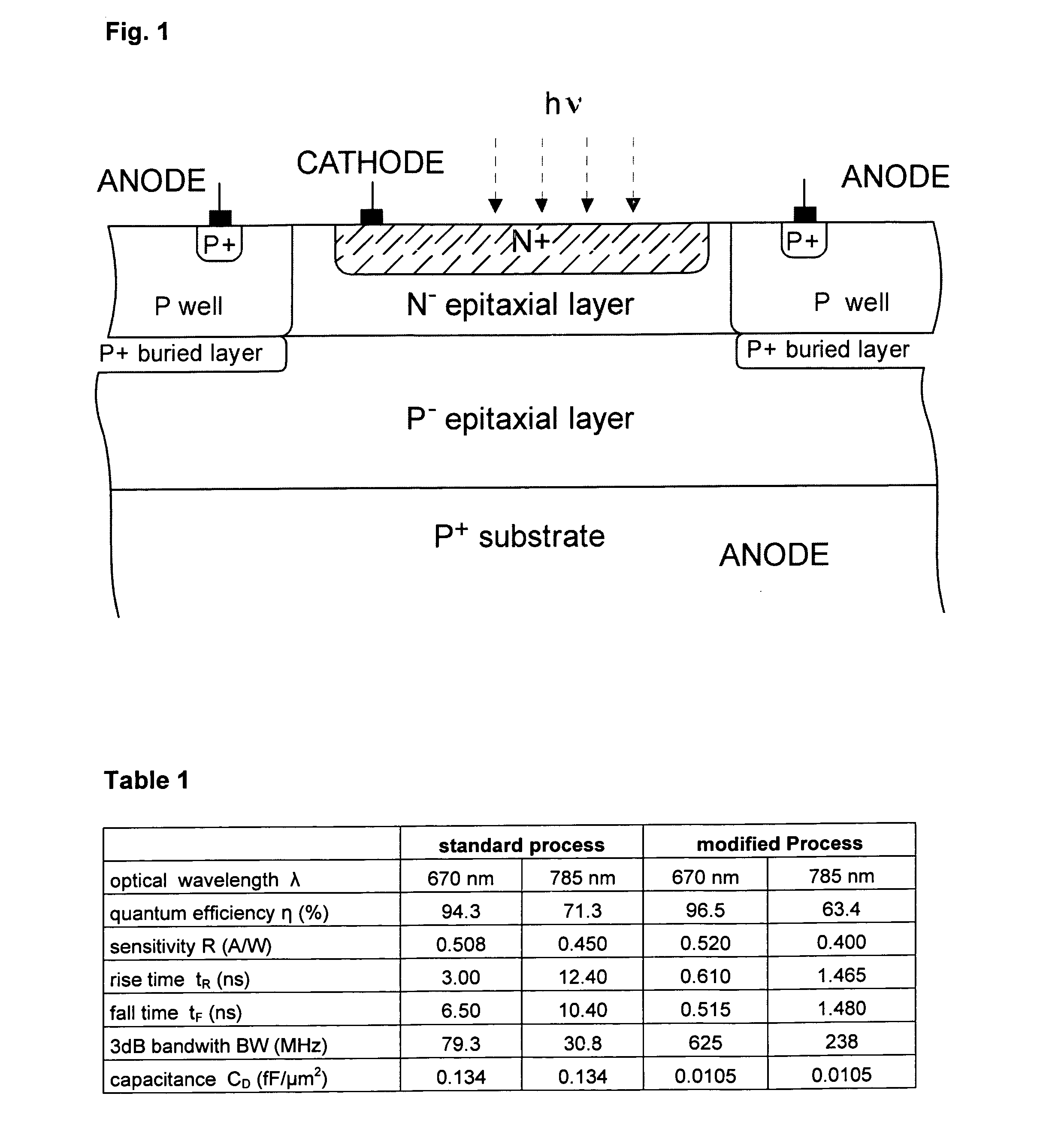
[0019] Table 1 includes the measurement results of photodiodes implemented by a non-modified and a modified biCMOS process, respectively. It is evident that according to the modification of the present invention for a wavelength of 670 nm, an integrated photodiode having a quantum efficiency of more than 95% may be obtained, wherein the short rise and fall times allow a processing bit rate of up to 1 Gbit / second. A reduced junction capacity CD allows for an increased photodiode area, which represents a further advantage.
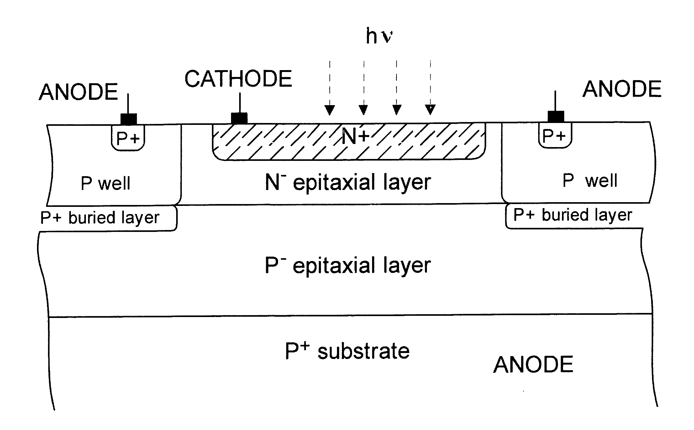
[0020]FIG. 1 illustrates the exemplary embodiment of a monolithically vertical PIN diode formed in biCMOS technology.
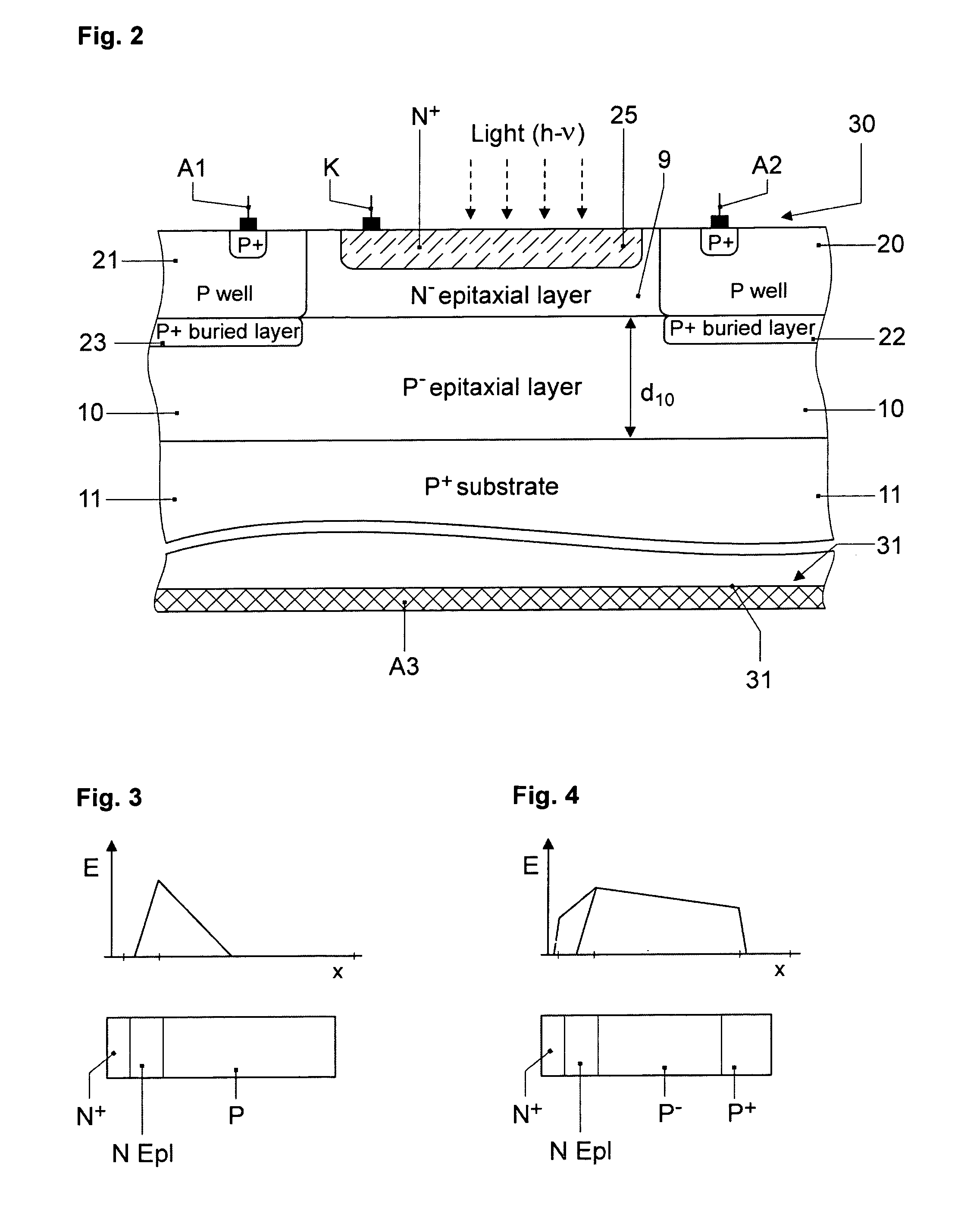
[0021] Existing layers and structures will be discussed in more detail with reference to a further illustrative embodiment according to FIG. 2. FIG. 2 represents a vertical structure of a PIN photodiode. The intrinsic i-zone is formed by two slightly doped epitaxially grown layers 9, 10. The layer following the substrate 11, is a p-type layer. The fu...
PUM
 Abstract
Description
Claims
Application Information