Forming method for film pattern, device, electro-optical apparatus, electronic apparatus, and manufacturing method for active matrix substrate

Inactive Publication Date: 2007-01-25
SEIKO EPSON CORP
View PDF9 Cites 43 Cited by
  • Summary
  • Abstract
  • Description
  • Claims
  • Application Information

AI Technical Summary

Benefits of technology

[0091] According to these manufacturing methods for an active matrix substrate, it is possible to form a high reliably active matrix substr

Problems solved by technology

In addition, there is a problem in the case in which a predetermined pattern including wirings or the like is formed by using such devices as described above, a complicated process is required, and the efficiency of utilization of the material is also only a few percent and almost all of the original material must be discarded so that the manufacturing cost increases.
However, in the pattern forming method which employs the above described liquid drop ejecting method, it has been difficult to form a minute pattern in a stable manner, because the liquid drops which have been ejected tend to spread out upon the substrate after ejected.
In particular, in the case in which the pattern is an electrically conductive film, accumulations of liquid (bulges) is occurred (formed) due to the above spreading out of the liquid drops, and there is concern that there is occurrence of some inconvenience such as broken wiring or short-circuiting or the like.
However, in the case in which the difference between the width of the minute wiring formation region and the width of the wiring formation region into which the functional liquid is ejected becomes large, since the functional liquid flows along the banks which demarcate the wide wiring formation region in generally, accordingly the amount of the functional liquid which flows into the minute wiring formation region due to the capillary phenomenon may be undesirably insufficiently.
Thus, there is a problem in that the thickness of the minute wiring pattern wh

Method used


Image

  • Forming method for film pattern, device, electro-optical apparatus, electronic apparatus, and manufacturing method for active matrix substrate
  • Forming method for film pattern, device, electro-optical apparatus, electronic apparatus, and manufacturing method for active matrix substrate
  • Forming method for film pattern, device, electro-optical apparatus, electronic apparatus, and manufacturing method for active matrix substrate

Examples


first embodiment

[0107] In the following, an embodiment of the invention will be explained with reference to the drawings.

[0108] The embodiments explained hereinafter are only for illustrating certain ways in which the invention may be implemented, and are not limitative of the invention.

[0109] Furthermore, in the drawings used in the following explanation, the scales of the various layers and the various members are changed as appropriate, in order to bring these layers and the members to sizes at which they may appear clearly in the drawings.

[0110] Liquid Drop Ejection Device

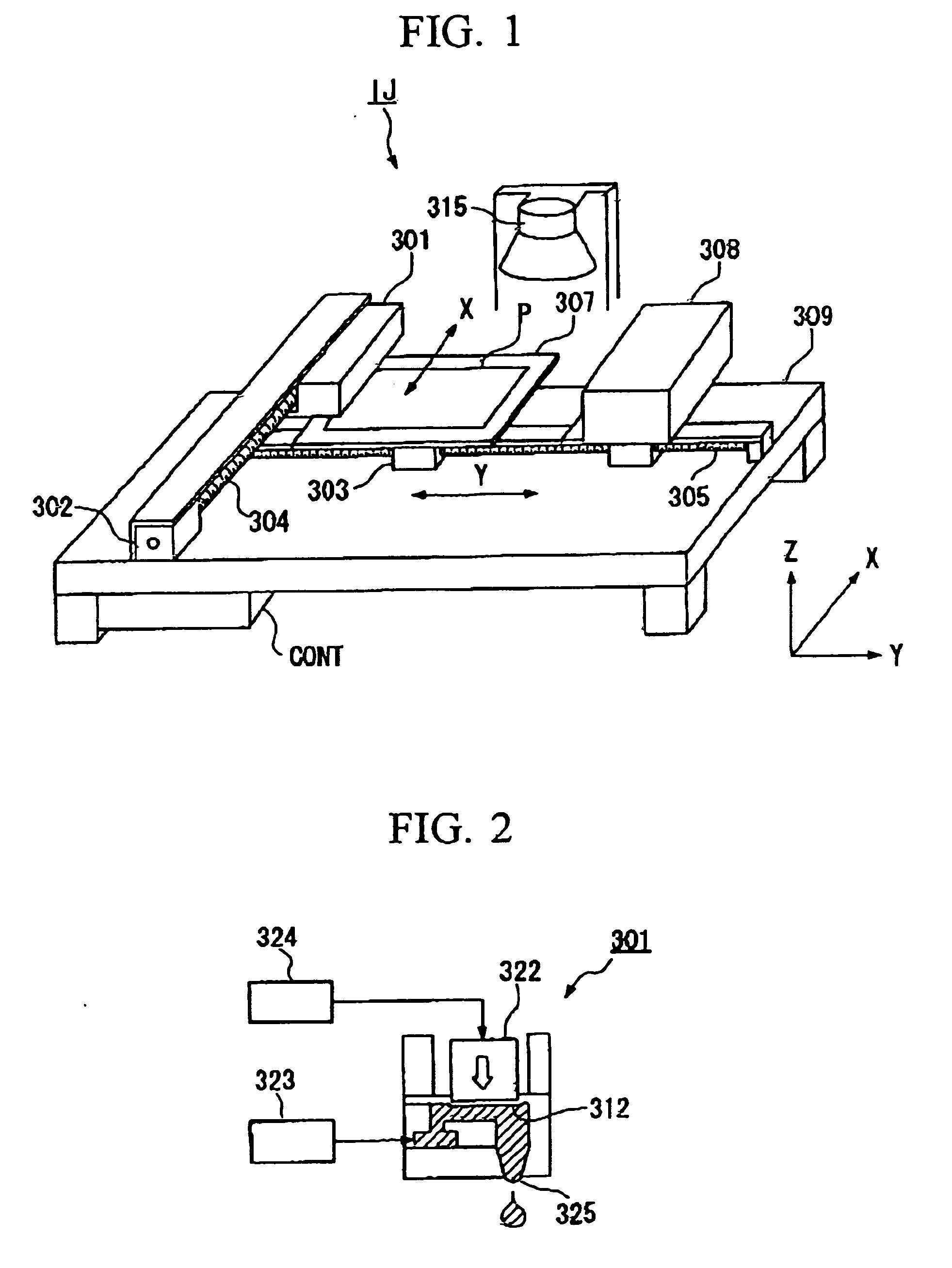
[0111] First, a liquid drop ejection device which is used for forming a film pattern will be explained with reference to FIG. 1.

[0112]FIG. 1 is a perspective view showing the schematic structure of a liquid drop ejection device (an ink-jet device) IJ. In the liquid drop ejection device IJ, liquid material is arranged upon a substrate by an ink drop ejecting method. This liquid drop ejection device IJ is one example of a d...

second embodiment

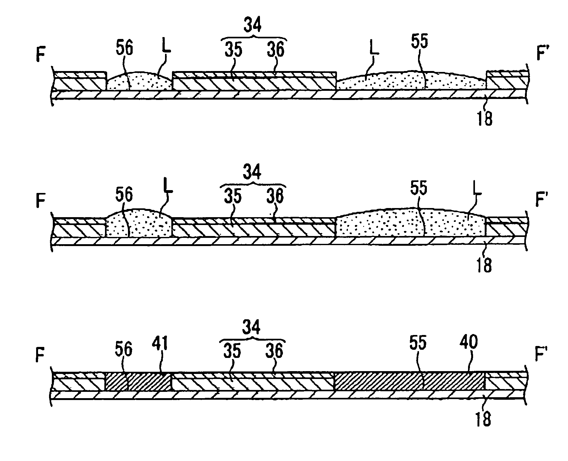
[0291] In the above described first embodiment, a case in which the film pattern is made from a single material was explained. The forming method for film pattern according to the invention is a forming method which also offers advantages, as compared with the prior art, in the case in which the film pattern is made as a multi-layered structure, from a plurality of different kind of material.

[0292] For example, in gate wiring which constitutes a pixel element of an electro-optical apparatus, there is a case in which a two-layered structure is employed.

[0293] This gate wiring includes a base layer which is made from at least one of metallic materials selected from Ag, Cu. Al and the like, and a covering layer which is made from at least one of metallic materials selected from Ni, Ti, W, Mn and the like.

[0294] By using of this two-layered structure, diffusion into the gate insulation layer of the Ag or Cu or Al included in the base layer is prevented by the covering layer, it is po...

third embodiment

[0301] Device

[0302] Next, a device incorporating a film pattern which has been formed with the forming method for the film pattern of the invention will be explained.

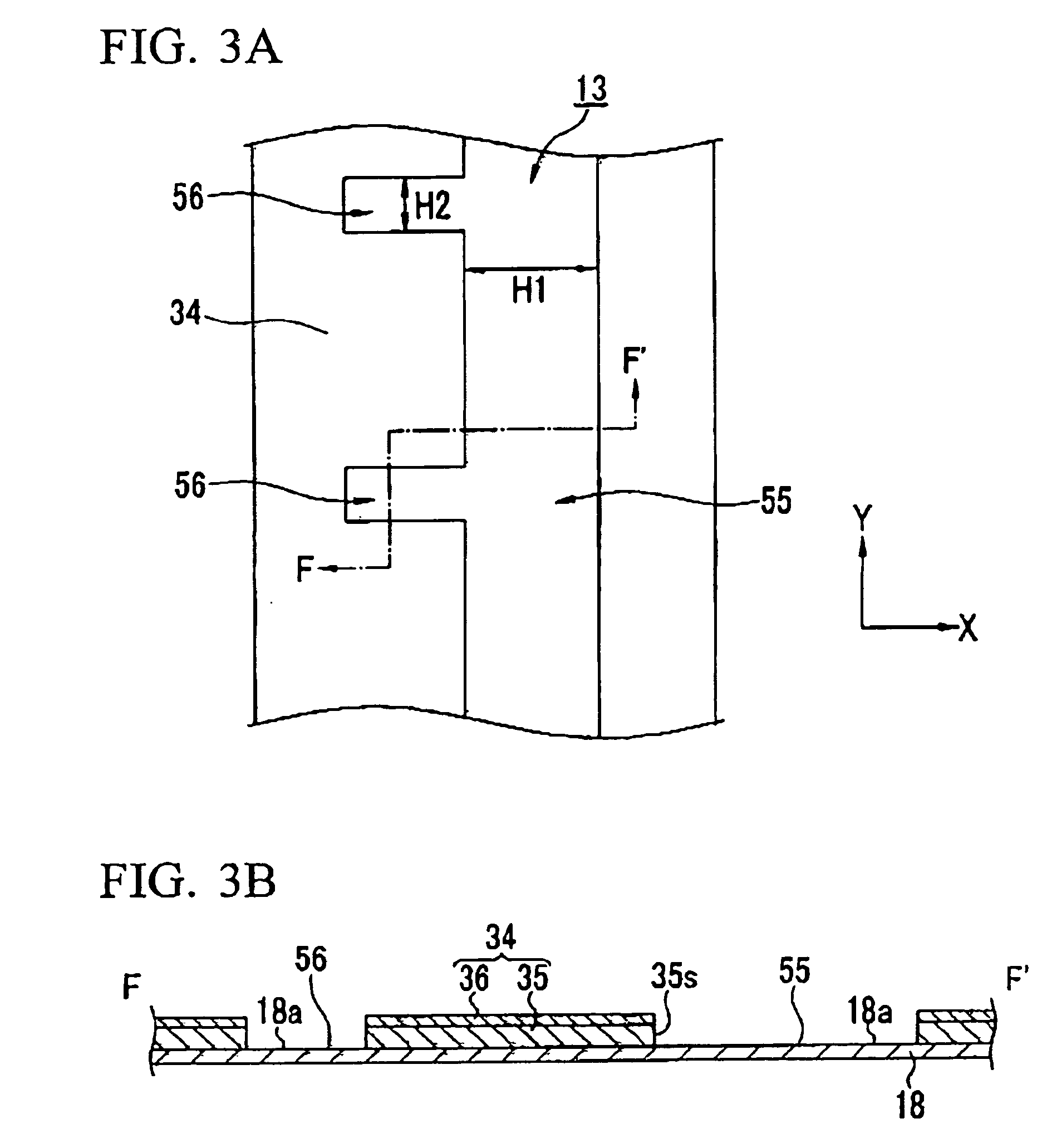
[0303] In this embodiment, a pixel element (a device) which incorporates gate wiring, and a manufacturing method for this pixel element, will be explained with reference to FIG. 7 and FIGS. 8A through 8E.

[0304] In this embodiment, a pixel element having a gate electrode, a source electrode, a drain electrode and the like of a TFT 30 of the bottom gate type is formed by employing the above described bank structure and forming method for film pattern .

[0305] In the following explanation, the description of processes which are the same as the layer formation processes in the first embodiment described above and shown in the above described FIGS. 5A, 5B, and 6A to 6C is curtailed.

[0306] Furthermore, to structural elements which correspond to structural elements shown for the first embodiment described above, the same r...


PUM


Abstract

A forming method for a film pattern, includes: forming a first bank layer on a substrate; forming a second bank layer on the first bank layer; patterning the first bank layer and the second bank layer thereby forming a bank having a pattern formation region including a first pattern formation region and a second pattern formation region which is connected to the first pattern formation region and has a width which is wider than that of the first pattern formation region; and forming the film pattern by depositing a functional liquid onto the pattern formation region which has been demarcated by the bank, wherein a first bank formation material and a second bank formation material are both materials including a siloxane bonds as a main chain, and the second bank formation material is a material including a fluorine bonds as a side chain.

Description

CROSS-REFERENCE TO RELATED APPLICATION [0001] This application claims priority on Japanese Patent Application No. 2005-210653, filed Jul. 20, 2005, and Japanese Patent Application No. 2006-080304, filed Mar. 23, 2006, the contents of which are incorporated herein by reference. BACKGROUND [0002] 1. Technical Field [0003] The present invention relates to a forming method for a film pattern, a device, an electro-optical apparatus, an electronic apparatus, and a manufacturing method for an active matrix substrate. [0004] 2. Related Art [0005] For example, a photolithographic method is widely used as a method for manufacturing wiring or the like which is to be arranged in a predetermined pattern for use in an electronic circuit or an integrated circuit or the like. [0006] In such a photolithographic method, large scale manufacturing devices such as a vacuum device, an exposure device, and the like are required. [0007] In addition, there is a problem in the case in which a predetermined p...

Claims


Application Information

Patent Timeline
IPC IPC(8): H01L21/20H01L21/44
CPCG02F2001/136295H01L21/02126H01L21/02216H01L21/02282H01L21/288H01L21/3122H01L27/1292H05K3/1241H05K3/1258H05K2203/0568H05K2203/0577H05K2203/1173H01L21/3127G02F1/136295H05K3/125H10K71/135
Inventor HIRAI, TOSHIMITSUMORIYA, KATSUYUKI
Owner SEIKO EPSON CORP
Why Eureka
Try Eureka