

Film taking-off method
a film and film technology, applied in the field of film production, can solve the problems of complex and expensive reclaiming operation proposed by u.s. patent no. 6,596,610, and may manifest particle contamination problems, and achieve the effects of simple and fast reclaiming operation, low cost, and good crystalline quality
- Summary
- Abstract
- Description
- Claims
- Application Information
AI Technical Summary
Benefits of technology
Problems solved by technology
Method used
Image

Examples
example 1
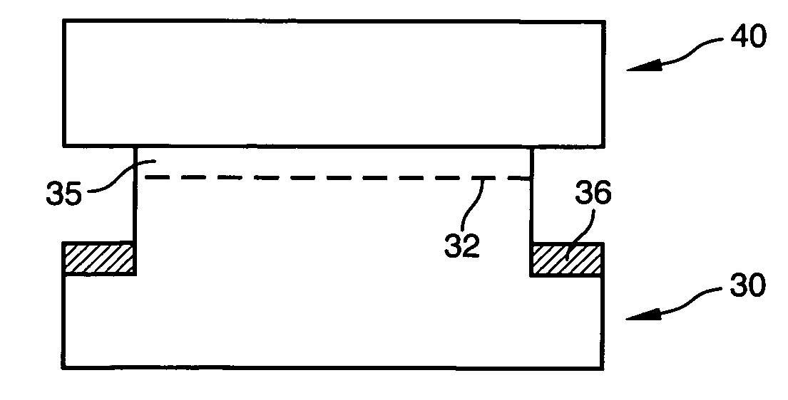
Formation of the Protective Layer 36
[0088] LPCVD deposition of a thin SiO2 layer;
[0089] anisotropic etching, such as RIE etching, in order to remove the protective material present on the front face 1.
example 2
Formation of the Protective Layer 36
[0090] PECVD deposition of SiO2 or Si3N4, optionally preceded by a thin thermal oxidation; a thickness of Rp+5*ΔRp (see above) or greater may be chosen. Thus, by adjusting the thickness of the layer 36′ it is possible to minimize the amount of material to be deposited, and therefore the cost of the operation; and
[0091] CMP (Chemical-Mechanical Planarization) polishing on at least the front face 1 in order to remove the SiO2 or Si3N4 layer selectively over the subjacent material.
example 3
Formation of the Protective Layer 36
[0092] thermal oxidation of the wafer 30; and
[0093] CMP polishing on at least the front face 1 in order to remove the SiO2 and Si3N4 layer selectively over the subjacent material.
PUM
 Abstract
Description
Claims
Application Information