Organic electroluminescent element and organic electroluminescent display device

Inactive Publication Date: 2007-02-01
SANYO ELECTRIC CO LTD
View PDF9 Cites 44 Cited by
  • Summary
  • Abstract
  • Description
  • Claims
  • Application Information

AI Technical Summary

Benefits of technology

[0112] The organic EL element of the first aspect of the invention is an organic EL element comprising a plurality of layered light emitting units and is capable of easily adjusting the cavity without changing the film thickness in the respective light emitting units. Accordingly, the organic EL element can be an organic EL element having a desired light emitting color and high light extraction quantity from the organic EL.
[0113] According to the second aspect of the invention, an organic EL element in which the cavity can be adjusted and which has a high light emitting efficiency, can lower the driving voltage, and can heighten the reliability and a

Problems solved by technology

However, since movement of a carrier in an organic EL element undergoes restriction due to an energy barrier between an electrode and an organic thin film, and low carrier mobility in an organic thin film, improvement in a light emitting efficiency is limited.
However, in the case of layering a plurality of light emitting layers, since a plurality of light emitting areas exist, there occurs a problem that the cavity adjustment becomes difficult.
However, there is a problem that when the thickness of the layers composing the each light emitting unit is adjusted, the carrier balance in each light emitting unit is changed to lead to the considerable alteration of the properties of the el

Method used


Image

  • Organic electroluminescent element and organic electroluminescent display device
  • Organic electroluminescent element and organic electroluminescent display device
  • Organic electroluminescent element and organic electroluminescent display device

Examples


examples 1 to 7 and reference examples 1 to 5

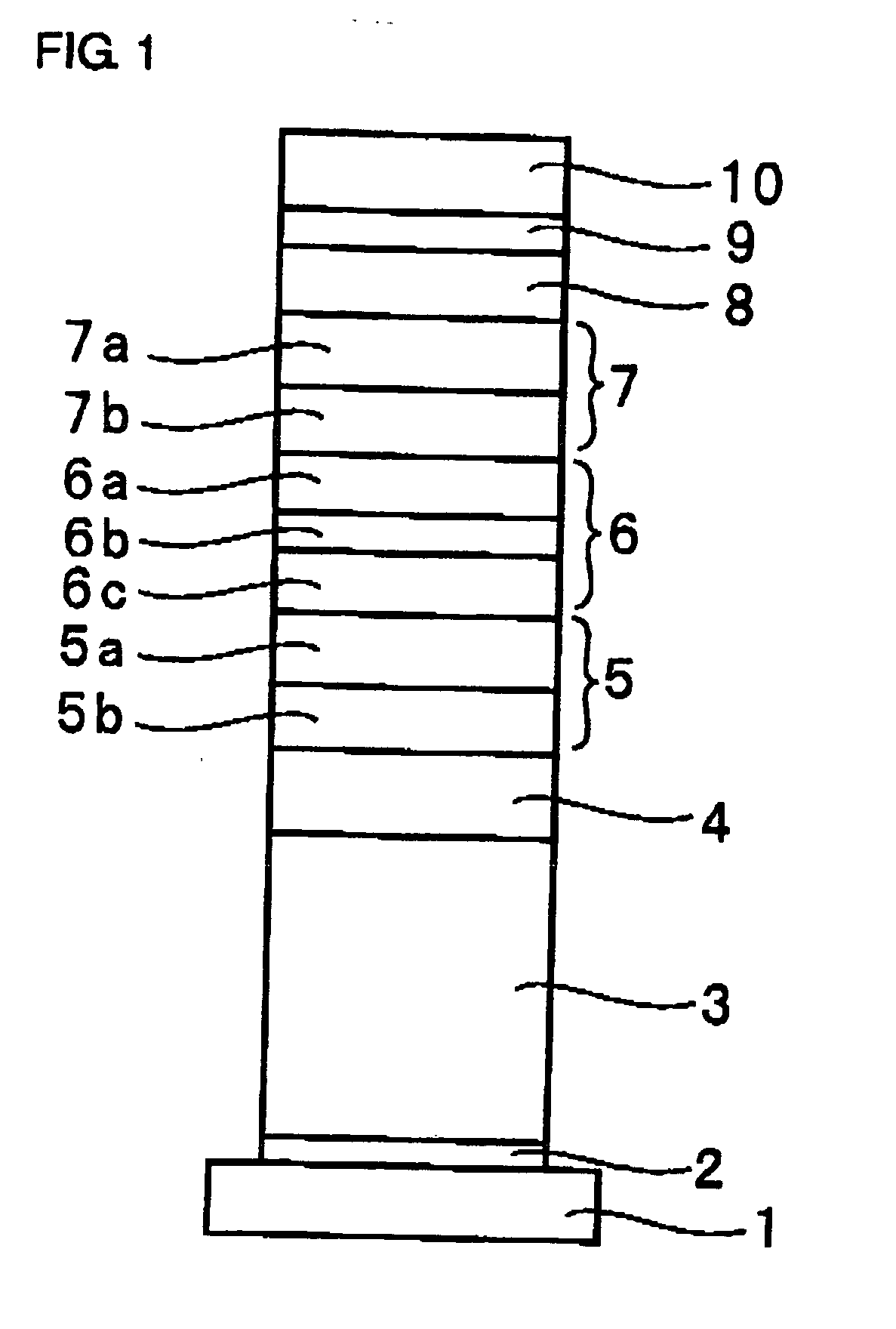
[0137] Organic EL elements of Examples 1 to 7 and Reference Examples 1 to 5 having the structure described with reference to FIG. 1 were fabricated. The compositions of the respective layers are as shown in Table 1.

TABLE 1SecondFirstHoleElectronCavityElectronInjectingExtractingAdjustmentExtractingFirst Light EmittingAnodeLayerLayerLayerLayerUnitIntermediate UnitITOCFxAs ShownAs ShownAs ShownNPB +TBADN +BCPLi2OHAT-in Table 2in Table 2in Table 220%10%(15)(0.5)CN6TBADN +NPB +(20)3% DBzR2% TBP(60)(50)ElectronElectronTransportingInjectingSecond Light Emitting UnitLayerLayerCathodeNPB +TBADN +BCPLiFAl20% TBADN +10% NPB +(15)(1)(200)3% DBzR2% TBP(60)(50)

[0138] A fluorocarbon layer, which is a hole injecting layer, was formed by plasma polymerization of CRF3 gas. The thickness of the fluorocarbon layer was adjusted to be 1 nm.

[0139] The cavity adjustment layer was formed using NPB, as shown in Table 2. NPB is N,N′-di(naphthacen-1-yl)-N,N′-diphenylbenzidine and has the following structure...

example 17

[0207]FIG. 9 is a schematic cross-sectional view showing an organic EL element fabricated in this example. In the organic EL element of this example, as shown in FIG. 9, a metal thin film 81 of Al is formed on a substrate, which is not illustrated and a transparent conductive film 82 (film thickness of 30 nm) of an ITO (indium tin oxide) film was formed thereon. A reflective electrode is composed of the transparent conductive film 82 and the metal thin film 81 and the upper surface of the metal thin film 81 is to be the reflection surface 41a.

[0208] A hole transporting layer 91 (film thickness of 30 nm) of NPB is formed on the transparent conductive film 82. The hole transporting layer 91 works as a first cavity adjustment layer.

[0209] An orange emitting layer 51 (film thickness of 60 nm) and a blue emitting layer 52 (film thickness of 50 nm) are layered in this order on the hole transporting layer 91. The first light emitting layer 50 is a white emitting layer composed of the ora...


PUM

PropertyMeasurementUnit
Fractionaaaaaaaaaa
Fractionaaaaaaaaaa
Fractionaaaaaaaaaa

Abstract

The invention provides an organic electroluminescent element comprising a cathode, an anode, a plurality of light emitting units layered and arranged between the cathode and the anode via an intermediate unit, a cavity adjustment layer formed between the light emitting unit nearest to the anode and the anode, and an electron extracting layer formed adjacently to the cavity adjustment layer in the light emitting unit side and is characterized in that the film thickness of the cavity adjustment layer is adjusted to adjust the optical distance from the light emitting position of each light emitting unit to the anode.

Description

BACKGROUND OF THE INVENTION [0001] 1. Field of the Invention [0002] The present invention relates to an organic electroluminescent element and an organic electroluminescent display device. [0003] 2. Description of the Related Art [0004] An organic electroluminescent element (organic EL element) has been actively developed from a viewpoint of application to display and illumination. Principle for driving an organic EL element is as follows; That is, a hole and an electron are injected through an anode and a cathode, respectively, these are transported in an organic thin film, and recombined in a light emitting layer to generate the excited state, and light emitting is obtained from this excited state. In order to enhance a light emitting efficiency, it is necessary to inject a hole and an electron effectively, and transport them in an organic thin film. However, since movement of a carrier in an organic EL element undergoes restriction due to an energy barrier between an electrode an...

Claims


Application Information

Patent Timeline
IPC IPC(8): H01L51/52H01L51/54H05B33/12
CPCC09K11/06C09K2211/1011C09K2211/1037C09K2211/1044C09K2211/186H01L27/322H01L51/5048H01L51/5265H01L51/5278H05B33/14H01L27/3244H10K59/38H10K59/12H10K50/14H10K50/852H10K50/19H05B33/22
Inventor NISHIMURA, KAZUKIHAMADA, YUJI
Owner SANYO ELECTRIC CO LTD
Why Eureka
Try Eureka