

Organic light emitting device and manufacturing method thereof
a light-emitting device and organic technology, applied in the direction of organic semiconductor devices, discharge tubes/lamp details, discharge tubes luminescnet screens, etc., can solve the problems of reducing the lifespan of the device, reducing the quantum efficiency of the organic light-emitting device, and high deviation in the number of excitons, so as to improve luminous efficiency and color stability, the effect of prolonging the li
- Summary
- Abstract
- Description
- Claims
- Application Information
AI Technical Summary
Benefits of technology
Problems solved by technology
Method used
Image

Examples
example 1
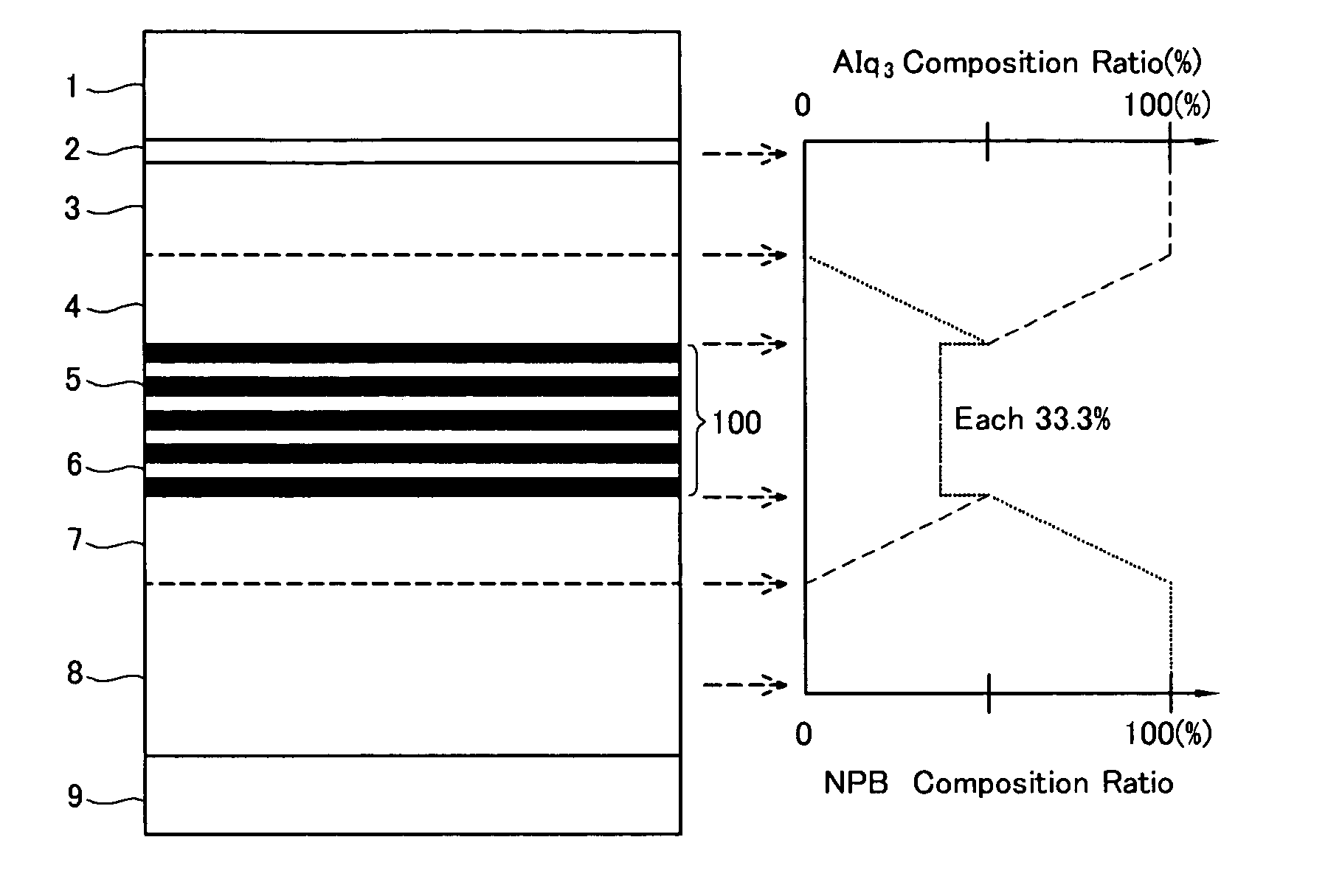
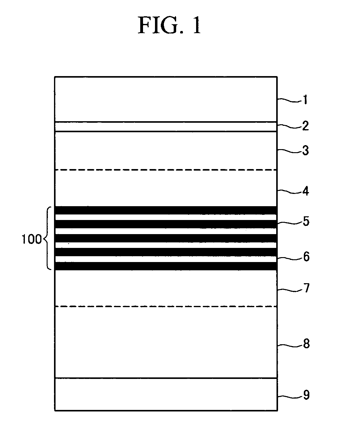
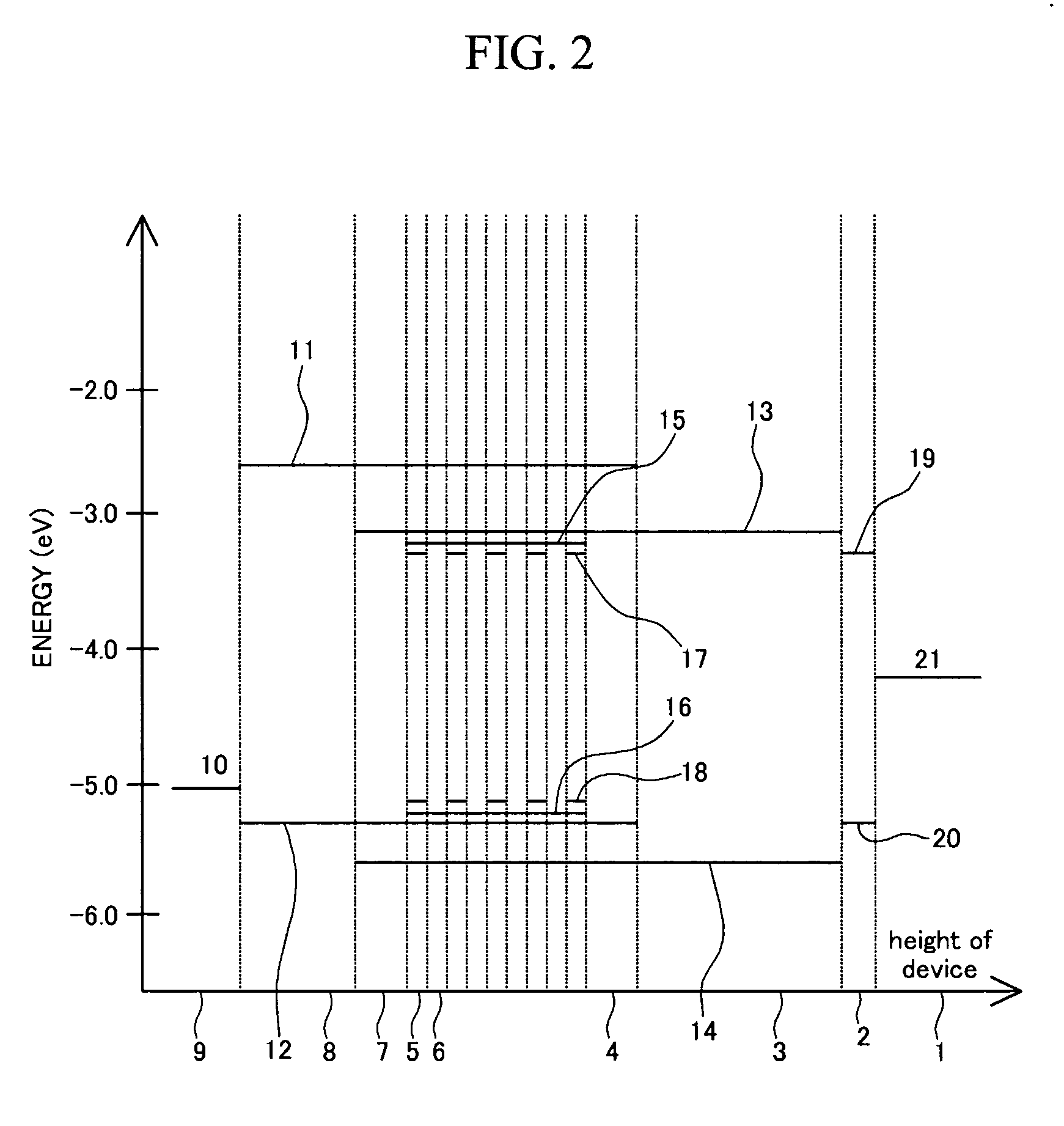
Manufacture of Organic Light Emitting Device Manufacture of Anode
[0062] An ITO thin film having a thickness of about 100 nm to about 150 nm and having a sheet resistance of about 30 Ω / cm2 was grown on a glass substrate (not shown) by deposition to form an anode 9.
[0063] Manufacture of Hole Transport Layer
[0064] NPB was deposited at 30 nm in thickness under a vacuum of about 10−7 Torr to about 10−9 Torr to form a hole transport layer 8. At this time, the growth rate was kept to be about 0.1 nm / seconds in order to grow a thin film of high quality.
[0065] Manufacture of First Stepwise Concentration Distribution Mixture Layer
[0066] A mixture layer 7 including NPB and Alq3 was deposited to a thickness of about 10 nm at a vacuum degree of about 10−7 Torr to about 10−9 Torr while gradually decreasing the growth rate of NPB, so that it transitioned from 1 Å / sec, to 0.9 Å / sec, to 0.8 Å / sec, and so on, and gradually increasing the growth rate of Alq3, so that it transitioned from 0 Å / sec...
experimental examples
Efficiency of Organic Light Emitting Device
[0075] Measured Current Density as a Function of Voltage in Organic Light Emitting Device
[0076] In addition to the organic light emitting device (denoted by Structure III) manufactured by the above-described method, a conventional organic light emitting device (denoted by Structure I) having hetero-junctions, and another organic light emitting device (denoted by Structure II) in which DCJTB was added into a host-mixture of NPB and Alq3 having a ratio of 1:1, but lacking a multiple quantum well film (e.g., the second mixture film 6), were fabricated. The organic light emitting device having Structure II also have hetero-junctions like Structure I. The above-described organic light emitting devices were made of substantially the same materials and had substantially the same structure except for the above-described features. In order to measure the efficiencies of the organic light emitting devices of the three structures, the current densit...
PUM
 Abstract
Description
Claims
Application Information